


How to Create a PCB Confirm Work File for Error-Free PCB Manufacturing
PCB manufacturing is a complex process that involves creating the physical foundation for electronic devices. The quality of the final product depends on several factors, with accuracy being crucial. Any mistake in design or production can lead to functional failures, delays, and increased costs. To avoid such issues, a PCB Confirm Work File plays a vital role. This file acts as a final checklist, ensuring that every detail of the design is correct before manufacturing begins. It includes essential documents like design files, material specifications, and production instructions, which help align the designer's intent with the manufacturer's capabilities.
The PCB Confirm Work File is the key to error-free production. It allows both designers and manufacturers to verify that the PCB design meets all requirements, ensuring that there are no misunderstandings or missed details. In this guide, we'll walk through the steps to create an effective PCB Confirm Work File, providing a structured approach to eliminate common production errors. By following this process, you can ensure a smooth manufacturing journey, reduce costly mistakes, and ultimately produce high-quality PCBs.
What is a PCB Confirm Work File and Why is it Essential for Error-Free PCB Manufacturing?
A PCB Confirm Work File is a comprehensive document that includes all necessary design and manufacturing details, ensuring alignment between designers and manufacturers to prevent errors and ensure accurate, cost-effective PCB production.
Definition of a PCB Confirm Work File
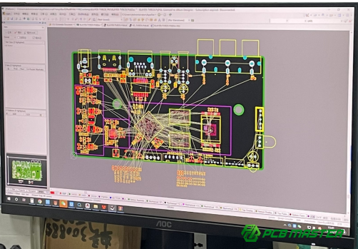
A PCB Confirm Work File is a comprehensive set of documents and files that ensure a PCB design is ready for manufacturing without errors. It acts as the final confirmation before production starts, aligning the design team's work with the manufacturer's capabilities. Typically, this file includes the PCB design files (such as Gerber files or ODB++ files), bill of materials (BOM), assembly instructions, material specifications, and any additional notes about special processes or components. This file serves as a checklist to confirm that every detail, from component placement to material selection, is correct before production begins.
The Importance of Confirming Work Files in PCB Production
The PCB Confirm Work File is essential because it ensures that designers and manufacturers are on the same page. When creating a PCB, designers might include very specific instructions that are not always clear or understood by the manufacturing team. The Confirm Work File bridges this gap by providing explicit and comprehensive details on every aspect of the design. This prevents errors that could arise from miscommunication, such as incorrect component placement or missing design elements.
Additionally, this file plays a crucial role in preventing design-to-production errors, which can be costly and time-consuming to fix. For instance, if a component's orientation is wrong or if traces are too close together, the board might not work as intended, leading to expensive revisions. A well-prepared work file ensures that everything is checked and verified in advance.
By using a Confirm Work File, the manufacturer can also ensure cost-efficiency. A smooth and error-free production process reduces waste and the need for rework, which can lower the overall cost of PCB manufacturing. This improves product quality, speeds up time-to-market, and enhances the reliability of the final product.
How to Gather and Organize Design Files for a PCB Confirm Work File?
To gather and organize design files for a PCB Confirm Work File, collect essential documents like schematics, layout files, BOM, and assembly drawings, include additional details like component placements and trace information, and organize the files using clear folder structures and consistent naming conventions for easy access.
Step 1: Collect Essential Design Documents
To create a comprehensive PCB Confirm Work File, start by gathering all the core design documents. These documents provide the necessary details for manufacturing the PCB accurately.
l PCB Schematics: The schematic diagram outlines the electrical connections of the components. It is essential for ensuring that the circuit works as intended and guides the PCB assembly process. This document is the blueprint for the circuit's functionality.
l Layout Design Files (Gerber, ODB++, etc.): These files contain the physical layout of the PCB, including the placement of traces, vias, and pads. Gerber files are the most common format for PCB manufacturing, while ODB++ is another widely used format that contains all design and manufacturing data in a single package. These files are crucial for transferring design data to the manufacturer.
l Bill of Materials (BOM): The BOM is a detailed list of all components used in the PCB design, including part numbers, quantities, and specifications. It helps ensure that the correct components are ordered and used during manufacturing.
l Assembly Drawings: Assembly drawings provide visual guidance on how components should be placed on the PCB. These drawings help manufacturers understand the component orientation, soldering guidelines, and any specific handling requirements for the components.
Step 2: Include Additional Important Information
Once the core design files are collected, include any additional information that may be critical for the manufacturer to ensure the PCB is made correctly.
l Component Placement and Footprint Details: These details specify where each component should be placed on the PCB. The footprint information defines the physical size and shape of each component to ensure that it fits properly on the board. If there are any special considerations for components (like specific pin orientations), they should be clearly noted here.
l Signal Layer and Trace Information: Including the signal layer information helps the manufacturer understand how signals will flow through the board. Trace widths, spacing, and routing details are important for ensuring the PCB meets electrical and thermal performance standards.
l Test Points and Unique Instructions: Test points are specific areas on the PCB where testing equipment can be attached to verify the circuit's functionality during manufacturing. If there are any special instructions, such as testing procedures or handling requirements for sensitive components, these should be added to prevent errors during assembly.
Step 3: Organize Files for Easy Access
Proper organization of the PCB design files is crucial for smooth collaboration between the design team and the manufacturer. Follow these best practices to ensure that the files are easy to access and manage:
l Best Practices for Folder Structures: Organize the files into clearly labeled folders based on their type, such as “Schematics,” “Layout Files,” “BOM,” and “Assembly Instructions.” This structure helps both the design team and the manufacturer quickly locate the necessary documents. A clean folder structure minimizes the risk of losing important files or mixing up documents.
l Naming Conventions for Files: Use consistent naming conventions to keep files easily identifiable. For example, use descriptive names like "Schematic_v1_2023" or "Gerber_RevA" instead of generic file names like "PCB1" or "file_1." This allows anyone working on the project to immediately understand what the file contains without opening it.
l Ensure Consistency Across All Related Design Documents: Consistency is key in maintaining a clear and organized PCB Confirm Work File. Ensure that all files are updated and match the latest version of the design. Also, ensure that the naming conventions, file formats, and folder structures are applied uniformly across all documents. Consistent documentation will minimize errors and confusion during the production process.
By following these steps, you will ensure that your PCB Confirm Work File is complete, organized, and easy to navigate, providing the manufacturer with all the necessary information to produce an error-free PCB.
How to Confirm Manufacturing Process Requirements in the PCB Confirm Work File?
To confirm manufacturing process requirements in the PCB Confirm Work File, define key production standards (e.g., material selection, layer stack-up, surface finish), provide detailed tolerances and clearances, and include specific fabrication and assembly instructions to ensure the design is accurately produced.
Step 1: Define Manufacturing Standards
To ensure a smooth and accurate manufacturing process, it's crucial to define the manufacturing standards clearly within the PCB Confirm Work File.
l Standard Production Techniques: This includes outlining key production methods such as layer stack-up, which defines how the layers of the PCB will be stacked and laminated. This ensures the design's structural integrity. For example, a typical stack-up might be 4-layer (Signal-Plane-Signal-Plane) or 6-layer based on the design’s complexity. It’s also essential to specify the solder mask type, which protects the PCB traces and helps prevent short circuits. Common options are green solder mask, though manufacturers may use other colors based on aesthetic or functional requirements.
l Material Selection: Materials must be specified clearly. For example, FR4 (a common PCB substrate material) is often used, but if the design requires something more specialized, like high-frequency substrates, it should be stated. Similarly, copper weight is crucial for the trace width and the current carrying capacity of the PCB. Standard copper weight is 1 oz/ft², but higher weights (e.g., 2 oz/ft²) may be needed for high-power circuits.
l Finish and Surface Treatment: Specify the required finish or surface treatment for the PCB, such as HASL (Hot Air Solder Leveling) or ENIG (Electroless Nickel Immersion Gold). These finishes impact solderability, durability, and even the final appearance of the PCB. For instance, ENIG is often chosen for precision applications due to its superior performance and reliability.
Step 2: Detail Tolerances and Clearances
Providing detailed tolerances and clearances ensures the PCB meets functional and manufacturing standards without failure.
l Tolerance Values: Tolerances define the permissible variations in the size of PCB features, such as hole sizes, trace widths, and component spacing. For example, hole sizes for vias should be within a certain range, typically ±0.1 mm, depending on the design and manufacturing capabilities. Similarly, trace widths must be accurately defined, especially for high-speed circuits, as they impact signal integrity.
l Clearance Requirements: Specific clearance values between traces, pads, and holes must be outlined to prevent electrical shorts or interference. For instance, a 0.2 mm minimum clearance might be required between traces on a high-density PCB to ensure reliable operation.
l Manufacturing Capability Limits: Each PCB manufacturer has different capability limits regarding tolerances and feature sizes. For instance, some manufacturers may not support hole sizes smaller than 0.2 mm or traces thinner than 0.1 mm. These limits should be confirmed in the work file to avoid incompatibilities between the design and the manufacturer’s equipment.
Step 3: Include Fabrication and Assembly Instructions
To avoid mistakes during PCB fabrication and assembly, include any specific instructions that guide the manufacturing process.
l Special Instructions for Components: Certain components, such as polarized capacitors or sensitive parts like LEDs, may require specific placement or handling instructions. For example, a component like a diode might need to be oriented in a specific direction, which should be highlighted in the work file.
l Layer-Specific Instructions: If the PCB design involves complex features like blind/buried vias or via-in-pad, these should be clearly noted. These features are often necessary for high-density designs but require special handling during fabrication. Blind vias, for example, only connect some layers of the PCB and require precision drilling, while buried vias do not go all the way through the board.
l Other Specific Requirements: For designs with high complexity, additional instructions might be necessary, such as specific testing procedures for circuit integrity or guidelines for component mounting on different layers of the PCB. If components are sensitive to heat or static, special handling precautions should also be included.
By clearly defining these manufacturing requirements, you ensure that the PCB production process is aligned with the design’s specifications, minimizing the risk of defects and delays. This level of detail in the PCB Confirm Work File will help the manufacturer produce a high-quality PCB that meets your design needs.
How to Validate the Accuracy of a PCB Confirm Work File Before Submission?
To validate the accuracy of a PCB Confirm Work File before submission, cross-check the design files against manufacturing specifications, review tolerances and material selections for compatibility, and use DFM guidelines to ensure the design is manufacturable with all necessary tests included.
Step 1: Cross-Check Design Files Against Specifications
Before submitting a PCB Confirm Work File, it is crucial to cross-check all design files with the intended manufacturing standards. This ensures that the design is aligned with the manufacturer's capabilities and avoids errors during production.
l Compare Design Files with Specifications: Review each file, such as schematics, layout designs, and BOM, to make sure they follow the intended manufacturing specifications. For example, verify that all components are correctly placed, and that the traces and pads are sized according to the manufacturer’s guidelines. If any discrepancies are found, it’s essential to correct them before moving forward.
l Ensure All Layers and Elements are Included: Double-check that all necessary design layers (e.g., signal, power, ground) are included in the files. Missing layers or incorrectly aligned layers can lead to serious production issues, such as improper routing or unconnected components. Make sure that all components and their connections are accurately represented and that there are no gaps in the design.
Step 2: Review Tolerances and Material Specifications
Tolerances and material specifications are essential to ensuring that the PCB is manufacturable and functions as expected.
l Ensure Tolerances Match Manufacturer’s Capabilities: Check that all the specified tolerances (e.g., hole sizes, trace widths) are within the manufacturer’s specified limits. For instance, some manufacturers may not be able to handle hole sizes smaller than 0.2mm or trace widths narrower than 0.1mm. Ensuring the design’s tolerances are compatible with the manufacturer’s capabilities reduces the risk of defects and delays.
l Double-Check Material Selection: Confirm that the materials selected (e.g., FR4, copper weight) are suitable for the design and that the manufacturer can source them. If the design requires specialized materials like high-frequency substrates or different copper weights, ensure the manufacturer can accommodate these materials and that they match the performance requirements of the PCB.
Step 3: Use DFM (Design for Manufacturability) Checklists
Design for Manufacturability (DFM) guidelines help ensure that the design is optimized for production, preventing manufacturing issues that could affect the PCB’s quality or functionality.
l Apply DFM Guidelines: Review the design using DFM guidelines to ensure it meets the manufacturer’s standards for production. For example, ensure that components are placed with adequate spacing, and that vias are correctly sized and positioned to avoid issues during the manufacturing process. DFM guidelines also help in identifying potential problems with the design, such as unbalanced layer stacking or complex geometries that could complicate fabrication.
l Confirm Necessary Tests Are Included: Verify that the work file includes all required tests to ensure the PCB’s quality. This could include electrical testing (to check for continuity and signal integrity) or mechanical checks (to confirm component fit and mounting). By including testing requirements, you can ensure that the final product meets the performance standards before it’s sent to production.
By thoroughly validating the PCB Confirm Work File through these steps, you reduce the likelihood of errors, ensuring that the manufacturing process runs smoothly and results in a high-quality PCB.
What Are Common Mistakes to Avoid When Creating a PCB Confirm Work File?
Common mistakes to avoid when creating a PCB Confirm Work File include missing or incomplete files, inaccurate tolerances and clearances, unclear manufacturing instructions, and failing to confirm details with the manufacturer.
Mistake 1: Missing or Incomplete Files
A common mistake when creating a PCB Confirm Work File is failing to include all necessary documents. This can cause significant delays in the manufacturing process and lead to costly errors.
l Importance of Including All Necessary Files: The work file should contain key documents such as schematics, layout files (Gerber, ODB++), Bill of Materials (BOM), and assembly drawings. These files provide the necessary information to the manufacturer, ensuring they can create the PCB correctly. Missing any of these documents could lead to incomplete or inaccurate PCB manufacturing, potentially halting production or requiring expensive rework.
l Consequences of Missing Files: If essential files are left out, the manufacturer might be forced to guess or make assumptions about the design, which increases the risk of mistakes. This can delay the production schedule, increase costs, and affect the overall product quality. For instance, if assembly drawings are missing, the manufacturer may place components incorrectly, leading to functionality issues.
Mistake 2: Inaccurate Tolerances and Clearances
Providing inaccurate or unclear tolerance and clearance information is another common mistake that can severely impact PCB production.
l Risks of Incorrect Tolerance Information: Tolerances define the allowable variations in PCB features, such as hole sizes, trace widths, and component spacing. If these tolerances are incorrect, it can lead to issues like poor soldering, unfit components, or failure to meet electrical performance standards. For example, traces that are too thin or holes that are too small can prevent the PCB from functioning correctly, especially in high-speed applications.
l How to Ensure Precise Measurements: To avoid this mistake, always double-check the tolerances and ensure they fall within the manufacturer’s capabilities. Use clear and standard measurement units, and be precise when specifying dimensions. For instance, if your design requires a 0.2 mm trace width, make sure it is specified accurately. Working with the manufacturer to verify tolerance limits can help prevent errors.
Mistake 3: Lack of Clear Manufacturing Instructions
Another mistake to avoid is the lack of clear manufacturing instructions in the PCB Confirm Work File.
l Importance of Providing Detailed Instructions: Clear, unambiguous manufacturing instructions ensure that the design is correctly understood and fabricated. These instructions should specify details like component orientation, special handling requirements, or special processes such as blind vias or via-in-pad. Without these details, manufacturers may make incorrect assumptions, leading to mistakes in assembly or fabrication.
l How Missing or Unclear Instructions Lead to Delays: Unclear instructions can result in misplacement of components, incorrect layer stacking, or failure to apply specialized processes. This can cause production delays, increased costs due to rework, and the risk of producing faulty PCBs. For example, if the component orientation for a polarized capacitor is not clearly indicated, the board may not function correctly when assembled.
Mistake 4: Not Confirming with the Manufacturer
A significant error that can be made during the creation of a PCB Confirm Work File is not confirming the details with the manufacturer before finalizing the design.
l How Direct Communication Helps Avoid Misunderstandings: Before submitting the work file, always engage in direct communication with the manufacturer to clarify any ambiguous parts of the design or file. Manufacturers may have specific capabilities or limitations, and discussing these beforehand ensures that the design matches what they can produce. It’s also important to verify that the file format is compatible with their system.
l Value of Design Reviews and Pre-Production Meetings: Conducting design reviews and pre-production meetings can help identify potential issues early on. These meetings allow the designer and manufacturer to review the design, discuss any potential challenges, and ensure all aspects of the PCB are ready for manufacturing. For example, confirming the material specifications and tolerances directly with the manufacturer can help prevent discrepancies during production.
Avoiding these common mistakes ensures that the PCB Confirm Work File is accurate, complete, and ready for a smooth and efficient manufacturing process. By ensuring that all files are included, tolerances are correct, instructions are clear, and communication with the manufacturer is established, you can minimize production errors and delays.
How to Ensure Effective Communication Between Designers and Manufacturers?
To ensure effective communication between designers and manufacturers, establish clear communication channels, use collaborative tools for sharing files and feedback, conduct regular design reviews, create pre-production checklists, and document all revisions and feedback clearly.
Step 1: Establish Clear Channels of Communication
To ensure smooth communication between designers and manufacturers, it is essential to establish clear channels of communication from the start.
l Importance of Regular Discussions: Regular conversations throughout the design process help ensure that both parties are aligned on project expectations, timelines, and requirements. When designers and manufacturers discuss the design, potential challenges can be identified early, allowing for adjustments before production begins. For example, if a designer realizes that a component cannot be sourced in time, they can quickly inform the manufacturer to find an alternative.
l Use of Collaborative Tools and Platforms: Collaborative tools, such as cloud-based platforms like Google Drive, Dropbox, or Trello, allow for easy sharing of files and feedback. These platforms enable both teams to access the most up-to-date documents and provide real-time comments. For example, designers can upload their PCB design files, and manufacturers can comment on specific areas that may need adjustments, such as component placement or trace width. This continuous feedback loop ensures that everyone has access to the same information and reduces the chance of errors.
Step 2: Perform Design Reviews and Pre-Production Checklists
Performing regular design reviews and using pre-production checklists help to verify that all details of the PCB are confirmed before manufacturing starts.
l Conducting Regular Design Reviews: A design review is a thorough inspection of the PCB design by both the design team and the manufacturer. This review ensures that the design meets all requirements and manufacturing capabilities. For instance, the designer might check for proper component placement, while the manufacturer could verify that the design adheres to their production constraints. Conducting these reviews early and often helps prevent costly mistakes and delays.
l Creating a Pre-Production Checklist: A pre-production checklist is a comprehensive list of all requirements and confirmations needed before starting PCB manufacturing. This checklist ensures that every detail, from material specifications to component orientations, is covered. For example, a checklist might include ensuring that the Gerber files are complete, the BOM is accurate, and the tolerances match the manufacturer’s capabilities. This final review confirms that everything is ready to move to production without overlooking critical steps.
Step 3: Document Feedback and Revisions Clearly
Clear documentation of feedback and revisions is essential for maintaining accurate records and ensuring that all parties are aligned.
l Record Revisions and Changes: Whenever feedback is provided, it is important to document any changes made to the design. For example, if the manufacturer suggests altering a trace width for manufacturability reasons, that change should be recorded and reflected in the updated files. This helps to ensure that the final design matches the agreed-upon specifications and avoids confusion down the line.
l Ensure Updates are Reflected in the Final PCB Confirm Work File: All revisions and changes should be incorporated into the final PCB Confirm Work File before submission. For example, if the manufacturer suggests a different layer stack-up, that change should be updated in both the design files and the work file. This ensures that the manufacturer is working with the most current and accurate information. Having a version control system in place also helps to keep track of changes and avoid mistakes in the final submission.
By following these steps to establish clear communication, perform regular reviews, and document feedback properly, designers and manufacturers can ensure a smooth and error-free PCB production process. These practices help catch potential issues early and ensure that the final product meets both design and manufacturing standards.
What Tools and Software Can Help in Creating and Managing a PCB Confirm Work File?
Tools like Altium Designer, Eagle, and KiCad for design, cloud-based file management tools like Google Drive and Dropbox for version control, and DFM/DFA tools like Valor NPI and SolidWorks PCB help create, manage, and optimize a PCB Confirm Work File for efficient and error-free manufacturing.
PCB Design Software Tools
PCB design software tools are essential for creating accurate PCB designs that can be used to generate the required files for manufacturing. Popular tools include Altium Designer, Eagle, and KiCad.
Overview of Popular Tools:
l Altium Designer is known for its advanced features, including high-speed design capabilities, robust component libraries, and seamless integration with manufacturing processes. It allows designers to create detailed PCB layouts and generate all necessary design files, including Gerber files and BOMs.
l Eagle is widely used by hobbyists and small businesses for its user-friendly interface and affordability. It supports key design features like schematics, PCB layout, and component libraries, making it a popular choice for simpler designs.
l KiCad is an open-source alternative that offers many of the features of commercial tools like Altium, including support for multi-layer designs and automatic generation of design files, all at no cost.
Integration Capabilities: These design tools can integrate with manufacturing partners to streamline the PCB production process. For example, Altium Designer allows direct export to formats compatible with PCB manufacturers, ensuring that the files provided to the manufacturer are accurate and up-to-date. Many tools also offer cloud-based collaboration features that allow for sharing files easily with manufacturers and receiving feedback.
File Management Software
Proper file management is critical for maintaining the integrity of the PCB design and ensuring smooth communication between design teams and manufacturers.
Cloud-Based Collaboration Tools:
Tools like Dropbox, Google Drive, and OneDrive allow for easy storage, sharing, and access to design files from anywhere. These platforms ensure that all team members and manufacturers are working from the latest version of the design files.
l Version Control: Using cloud-based file management software helps in keeping track of changes over time. For instance, Google Drive automatically saves versions of documents, allowing you to revert to previous versions if needed. This version control feature is vital when multiple team members or manufacturers are making edits or providing feedback, as it ensures that no changes are lost and all revisions are documented.
Importance of Version Control: Version control helps maintain a clear history of design changes, allowing both designers and manufacturers to track modifications and understand the rationale behind specific updates. It minimizes the risk of errors due to using outdated files, making it essential for keeping the PCB Confirm Work File consistent and accurate.
DFM and DFA Tools
Design for Manufacturability (DFM) and Design for Assembly (DFA) tools help ensure that the PCB design can be manufactured and assembled without issues, reducing the likelihood of errors during production.
Tools for Checking DFM and DFA:
l DFM Tools: These tools analyze the design to ensure that it can be manufactured efficiently. They check for issues like trace widths that are too small, hole sizes that cannot be drilled, or layers that are improperly stacked. Popular DFM tools include Valor NPI, Autodesk Fusion 360, and Zuken CR-8000.
l DFA Tools: DFA tools focus on optimizing the PCB design for easy assembly. They check for things like component placement efficiency, the accessibility of components for soldering, and whether components are correctly oriented. Tools like SolidWorks PCB and Mentor Graphics can help designers optimize their designs for easier and more cost-effective assembly.
How These Tools Streamline Manufacturing: By identifying potential issues early in the design process, DFM and DFA tools help prevent costly revisions and manufacturing delays. For instance, if a DFM tool detects that a trace is too narrow for the chosen PCB thickness, it allows the designer to correct the issue before sending the design to production. Similarly, DFA tools ensure that components are placed in a way that minimizes errors during assembly, which can reduce rework and improve the overall efficiency of the production process.
By using the right design software, file management systems, and DFM/DFA tools, designers can create and manage a PCB Confirm Work File that is not only accurate but also optimized for a smooth and error-free manufacturing process. These tools help streamline communication with manufacturers, track revisions, and ensure that the design is ready for successful production.
Conclusion
Creating a well-structured and accurate PCB Confirm Work File is crucial for ensuring that your PCB design transitions smoothly into production. By carefully organizing design files, confirming manufacturing process requirements, and maintaining clear communication with manufacturers, you can significantly reduce the risk of production errors. This process not only minimizes costly mistakes but also improves the efficiency of the manufacturing process, ultimately saving time and money.
Following these steps helps ensure that every detail is covered, from design accuracy to material specifications, leading to a more reliable end product. Clear documentation, such as the PCB Confirm Work File, streamlines collaboration, helping both designers and manufacturers work together seamlessly. For companies seeking to ensure top-quality PCBs and PCBA (Printed Circuit Board Assembly), working with an experienced supplier like PCBMASTER can be an excellent choice. As a seasoned provider in the PCB industry, PCBMASTER is committed to delivering high-quality products and supporting users through every step of the design and manufacturing process, ensuring the best results for each project.
FAQs
1. What is the difference between a PCB Confirm Work File and a standard PCB design file?
A PCB Confirm Work File goes beyond a standard PCB design file by including not only the layout and schematic information but also all the additional documents and detailed instructions necessary for manufacturing. While a standard PCB design file typically consists of the schematic diagram, PCB layout (including Gerber files), and sometimes a Bill of Materials (BOM), a PCB Confirm Work File includes those elements plus crucial manufacturing details. These can include layer stack-up, material specifications, tolerances, clearances, assembly instructions, and any other specific requirements for fabrication and assembly. The purpose of the Confirm Work File is to ensure that all parties involved in the production process are aligned and that no critical information is missing, which helps prevent manufacturing errors and delays.
2. Can I use automated tools to generate a PCB Confirm Work File?
Yes, many PCB design software tools like Altium Designer, Eagle, and KiCad offer integrated features that allow designers to automatically generate PCB Confirm Work Files or at least assist in generating key documents such as Gerber files, BOMs, and assembly drawings. However, while these tools can create the bulk of the work file, manual review and verification are crucial to ensure that everything is accurate and up-to-date. Automated tools can help in the generation of required files, but they do not replace the need for human oversight. For example, designers must ensure that all special instructions, like tolerances or material specifications, are correctly added and that files are in the correct format for the manufacturer.
3. How often should I update the PCB Confirm Work File?
The PCB Confirm Work File should be updated whenever there are significant changes in the design, materials, or manufacturing process. For instance, if you change the layout, update the component selection, or modify the tolerances or assembly instructions, these updates should be reflected in the work file. Frequent updates ensure that the manufacturer always has the most accurate and current information to avoid potential errors during production. If you modify the design or make any last-minute changes, don’t forget to update the work file to ensure that all necessary documents are included. This continuous update process is especially important in dynamic, fast-paced design cycles where multiple iterations might occur.
4. Is it necessary to communicate directly with the manufacturer before submitting a PCB Confirm Work File?
Yes, direct communication with the manufacturer is highly recommended and plays a critical role in ensuring that your PCB design is manufacturable. Discussing the design specifications, materials, tolerances, and other important details ensures that the manufacturer fully understands your requirements and confirms their ability to meet them. For example, the manufacturer may have specific requirements or limitations on trace widths, hole sizes, or material selection that could affect the design. A direct conversation helps to avoid misunderstandings and ensures that both the designer and manufacturer are on the same page before production begins. Additionally, a design review meeting with the manufacturer can help catch potential issues early on, which saves time and money in the long run.
5. What happens if a PCB Confirm Work File is not properly created or checked?
If a PCB Confirm Work File is not properly created or thoroughly checked, it can lead to a host of problems during the manufacturing process. Missing or incomplete files, inaccurate tolerances, or unclear manufacturing instructions can cause production errors, leading to defective PCBs or delays. For example, if assembly instructions are omitted or unclear, components might be placed incorrectly, which could cause the PCB to malfunction. Similarly, failure to update the file after design changes can result in using outdated files, leading to manufacturing defects or costly rework. In some cases, improper files can delay production, increase costs, and even result in a failed final product that does not meet the customer’s specifications, ultimately harming the reputation and financial performance of both the designer and manufacturer. Therefore, ensuring the accuracy and completeness of the PCB Confirm Work File is critical for smooth, cost-efficient production.
Author Bio
Hi, I'm Carol, the Overseas Marketing Manager at PCBMASTER, where I focus on expanding international markets and researching PCB and PCBA solutions. Since 2020, I've been deeply involved in helping our company collaborate with global clients, addressing their technical and production needs in the PCB and PCBA sectors. Over these years, I've gained extensive experience and developed a deeper understanding of industry trends, challenges, and technological innovations.
Outside of work, I'm passionate about writing and enjoy sharing industry insights, market developments, and practical tips through my blog. I hope my posts can help you better understand the PCB and PCBA industries and maybe even offer some valuable takeaways. Of course, if you have any thoughts or questions, feel free to leave a comment below—I'd love to hear from you and discuss further!

