


Understanding PCB Line Graphics: Key Terms and Techniques for Effective Design
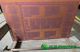
The line patterning process in PCB manufacturing is essential for defining the conductive pathways on a circuit board. This step transfers the circuit design onto a copper-clad substrate, forming the electrical traces that connect various components. The precision of this process significantly impacts the overall performance and reliability of the finished PCB.
The process begins with preparation, where tools like photomasks (films) and copper oxidation treatments are used to set the foundation. During the pattern formation stage, a light-sensitive resist layer is applied, exposed to UV light through the photomask, and developed to reveal the circuit design. Finally, etching removes unwanted copper, leaving behind the precise traces needed for the board’s functionality.
Understanding terms like "photomasks," "etching," and "copper oxidation" is key to grasping how the line patterning process works. These terms describe critical actions and materials that ensure the PCB is crafted with accuracy, providing the necessary electrical connections for electronic devices.
Graphic Transfer Preparation Phase: How to Prepare for Line Pattern Formation?
The graphic transfer preparation phase involves using photomasks (films) and copper oxidation treatments to lay the foundation for transferring the circuit design onto the PCB.
1. What is a Photomask/Film?
A photomask (or film) is a crucial tool used in PCB manufacturing to transfer the circuit design onto the copper substrate. It acts like a stencil that blocks light in specific areas, allowing only the desired patterns to be exposed during the process. The photomask is typically made of transparent material with opaque sections where the circuit design will be.
There are two main types of photomasks: positive and negative. A positive film has the circuit pattern in black, which blocks light, while a negative film has the pattern in clear areas, allowing light to pass through. In the exposure process, the positive or negative mask will dictate which parts of the photoresist layer will harden (positive) or remain soluble (negative), guiding the etching process later.
In the graphic transfer phase, the photomask is carefully aligned with the copper-clad PCB and exposed to UV light. The design transferred through the film is critical to ensure accuracy and precision in the final PCB pattern.
2. What is Black/Brown Oxidation and How Does It Help?
Black oxidation and brown oxidation are treatments applied to the copper surface of the PCB to improve its bond with the prepreg (a partially cured resin sheet) and to enhance the board’s resistance to high temperatures. These oxidation treatments involve creating a thin layer of oxidized copper on the surface, which provides a rougher texture.
The purpose of oxidation is twofold: first, it increases the adhesion between the copper layer and the prepreg, ensuring a stronger bond during lamination. Second, it improves the board’s high-temperature resistance, reducing the risk of delamination (separation of layers) during manufacturing or in the final usage of the PCB.
This step is especially important for multilayer PCBs, where the layers need to be securely bonded to each other to prevent structural failure. Oxidation improves the reliability and longevity of the PCB, making it suitable for high-performance applications in industries like automotive and telecommunications.
Graphic Formation Phase: How Are PCB Line Patterns Formed?
The graphic formation phase involves applying a light-sensitive resist layer, exposing it to UV light, developing the resist, etching the copper, and stripping away the remaining resist to form precise circuit patterns on the PCB.
1. How Does the Coating/Film Application Process Work (Dry Film & Wet Film)?
Dry Film and Wet Film are two methods used to apply a light-sensitive resist layer onto the copper surface of a PCB. Dry Film involves placing a solid, pre-made light-sensitive film onto the PCB using heat and pressure, while Wet Film is a liquid photoresist that is applied using roller coating, curtain coating, or spraying. Both methods are used to create a protective layer that will define the circuit pattern during the exposure and etching processes.
The process of applying the resist layer involves evenly coating the copper surface with either dry or wet film. In Dry Film, the film is heated and pressed onto the PCB, adhering tightly to the surface. In Wet Film, the liquid resist is spread across the surface and then dried in an oven. The resist layer is crucial because it will protect certain parts of the copper from the etching chemicals in the next stage.
Common problems in this process include uneven coating, bubbles trapped under the film, or poor adhesion, which can affect the final quality of the PCB.
2. How Does Exposure Affect the Formation of Line Patterns?
Exposure involves shining UV light through a photomask onto the resist-coated PCB. The purpose of exposure is to activate the light-sensitive properties of the resist. The UV light will either harden the resist (in a positive photoresist process) or leave the exposed areas soluble (in a negative photoresist process). This allows the desired pattern to be transferred onto the resist layer.
In the exposure process, precision is key. The alignment of the photomask with the PCB must be perfect to ensure that the circuit pattern is accurately transferred. If the exposure time or intensity is incorrect, it can lead to misalignment or incomplete exposure, which can ruin the design and affect the functionality of the PCB.
Exposure requires careful control of the light's intensity and duration to achieve accurate pattern formation.
3. How Does Developing Remove Unexposed Photoresist?
The developing process uses a chemical solution to remove the areas of photoresist that were not exposed to UV light. The developing solution dissolves the resist in areas where the light didn’t harden it, revealing the copper surface beneath. This step is crucial to creating the correct circuit pattern, as it defines the final layout of the PCB.
After the resist has been exposed to UV light, it is placed in a developing solution, which can be a weak alkaline solution or a specific developer designed for the photoresist used. The developing solution will dissolve the unexposed photoresist, leaving only the areas that were exposed to UV light. The result is a pattern that mirrors the photomask.
To ensure precision, it's important to carefully control the developing time and solution concentration. Overdeveloping or underdeveloping can result in inaccurate patterns.
4. How is a Stable Line Pattern Formed During Etching?
Etching is the process used to remove unwanted copper from the PCB, leaving behind the desired circuit lines. This is done by applying a chemical etchant that dissolves the copper in unprotected areas. Etching essentially "carves" the circuit pattern into the copper layer, creating conductive pathways for electrical connections.
To avoid undercut (where the etching fluid erodes the edges of the circuit pattern, causing the lines to widen), controlling the etching depth and width is essential. The etching factor, which measures the etch depth relative to the line width, helps ensure high-quality etching. Proper control of the etchant concentration, temperature, and exposure time is crucial for achieving precise and consistent line patterns.
Common problems during etching include over-etching, which can thin out lines, and under-etching, which leaves copper in unwanted areas.
5. What is the Purpose of Stripping the Resist?
Stripping, or removing the resist, is the final step in the graphic transfer process. After the etching process is complete, the remaining photoresist, which has protected the copper that was not etched, must be removed. This is done by using a strong alkaline solution to break down and remove the resist layer.
The stripping process is important because it ensures that only the copper traces remain on the PCB, leaving a clean and precise circuit pattern. If the resist is not completely removed, it can interfere with subsequent steps like soldering or assembly.
The stripping solution is carefully applied to dissolve the remaining resist without damaging the underlying copper traces. This ensures that the final PCB is fully functional, with a clean and intact circuit pattern ready for further processing or component mounting.
Special Processes and Related Terminology: What Are the Special Techniques in Line Pattern Formation?
Special techniques like the half additive method, line compensation, and teardrop design are used to optimize PCB manufacturing, ensuring precision, strength, and reliability in the final circuit patterns.
1. What is the Difference Between the Half Additive Method and the Subtractive Method?
The Subtractive Method is the traditional way of manufacturing PCBs. It starts with a copper-clad board, and unwanted copper is removed through the process of etching, leaving the desired circuit pattern. This method is simple and widely used, especially for single-layer PCBs. The main challenge is to accurately remove copper without damaging the traces or leaving unwanted copper behind.
The Half Additive Method combines both additive and subtractive processes. It begins by applying a thin layer of copper to the insulating substrate using chemical deposition. Then, the circuit design is formed by electroplating copper onto the areas that need to be thicker. Afterward, excess copper is removed by etching. This method is ideal for more complex designs and multilayer PCBs, as it allows for greater control over the thickness of the copper traces.
In terms of PCB manufacturing choices, the subtractive method is cost-effective for simpler designs, while the half additive method is often used for more advanced and intricate PCBs that require higher precision and better control of trace thickness.
2. How Does Line Compensation Optimize PCB Design?
Line compensation is a technique used to adjust the width of the PCB traces before manufacturing to account for the natural variations that occur during the etching and plating processes. The goal is to ensure that after the manufacturing process, the actual line width matches the design specifications.
The purpose of line compensation is to account for factors such as etching undercut (where the sides of the trace are eroded), plating thickness variations, and other process-induced changes. By widening the trace width slightly during the design phase, manufacturers can ensure the final PCB lines maintain the required electrical performance.
Adjusting the trace width can affect the precision of the final product. For instance, if the traces are too narrow after compensation, they may not carry enough current, while traces that are too wide could lead to wasted space on the board. Line compensation ensures that the finished PCB meets the design’s electrical requirements and mechanical constraints, leading to a more reliable and accurate final product.
3. Why is Teardrop Design Important for PCB Layout?
Teardrop design is a technique used in PCB design to strengthen the connection between traces and pads. It involves adding a smooth, curved transition (shaped like a teardrop) between a trace and a pad. This design improves the mechanical strength of the PCB and reduces the risk of breakage or failure in the connection, especially during the drilling or soldering process.
The teardrop shape is used at points where the trace meets the pad, which are often weak spots where stress can cause the PCB to fail. By making the transition more gradual, the design reduces stress concentration, making the PCB more durable and reliable.
In terms of mechanical strength and anti-fracture capability, teardrop designs are particularly important for PCBs that will face high vibration or mechanical stress. These designs are commonly seen in automotive, aerospace, and consumer electronics where durability is key.
Common Defects and Issues: What Defects Can Occur in the Line Patterning Process?
Defects such as line gaps, pinholes, short circuits, open circuits, residual copper, and exposure issues can occur during the PCB line patterning process, affecting the quality and functionality of the final circuit board.
1. How Do Line Gaps and Pinhole Defects Occur?
Line Gaps are small interruptions or breaks in the copper traces that can occur during the etching process, when the copper is not fully removed or when the photoresist does not protect the copper in certain areas. This defect can cause the circuit to be incomplete, leading to potential issues with electrical connectivity. Solutions include improving the quality of the resist layer, ensuring correct exposure times, and fine-tuning the etching process to avoid over-etching.
Pinhole Defects are tiny holes that can form in the copper layer due to contamination or improper etching conditions. These defects can lead to short circuits or loss of signal. Prevention involves ensuring clean equipment and surfaces, controlling etching parameters, and inspecting the resist layer for uniformity before exposure. Using high-quality materials can also minimize the risk of pinholes.
2. How Can Short Circuits and Bridging Issues Be Prevented?
Short Circuits and Bridging occur when two unintended copper traces connect, creating a direct path for electrical current where it should not be. This can happen due to issues in the etching process, where the copper lines become too close together, or due to incorrect mask alignment during the exposure stage. Best practices for preventing short circuits and bridging include ensuring proper trace spacing, using high-precision photomasks, and fine-tuning the etching process to prevent unwanted copper connections.
In addition, using design rules that maintain safe trace widths and clearances helps avoid these defects. Regular inspections and tests, such as electrical testing during manufacturing, can catch these issues before the PCB is finalized.
3. What Causes Open Circuits and How to Avoid Them?
Open Circuits or Broken Traces occur when there is a break in the copper trace, preventing the electrical current from flowing properly. This can be caused by over-etching, where the copper is removed too aggressively, or by poor photomask alignment during the exposure process. To prevent open circuits, manufacturers must carefully control the etching time, use accurate photomask registration, and regularly inspect the traces during manufacturing.
Process control such as etching rate optimization and pre-emptive testing can identify areas where the copper is thinning too much. Additionally, visual inspections during production can catch potential issues before they affect the functionality of the PCB.
4. How to Resolve Residual Copper Problems?
Residual Copper refers to leftover copper in areas where it should have been etched away, leaving unwanted copper "dots" or traces. This can happen when the etching process is incomplete, or when the resist layer does not protect the copper adequately. To resolve this, manufacturers can improve their etching process, use more effective etching chemicals, and ensure uniform resist application to ensure that all unwanted copper is removed.
During inspection, residual copper can be detected through visual or automated testing methods like X-ray inspection. Once detected, these areas can be removed through additional etching or a cleaning process.
5. How Do Exposure Issues and Photomask Scratches Affect Pattern Accuracy?
Exposure Problems arise when the photoresist does not react properly to the UV light, which can happen due to issues like improper exposure time, incorrect intensity of UV light, or misalignment of the photomask. This can lead to inaccurate pattern transfer and affect the quality of the PCB. To solve this, careful control of the exposure parameters and precise alignment of the photomask are critical.
Photomask Scratches can distort the design pattern by allowing light to pass through unintended areas. Scratches can be caused by improper handling or damage during storage or processing. Prevention involves using high-quality photomasks, ensuring proper handling, and inspecting them for damage before use. Scratched masks should be replaced to avoid pattern errors.
Proper exposure and photomask maintenance are crucial for maintaining the accuracy and functionality of the final PCB design.
Conclusion
The PCB line patterning process plays a crucial role in determining the quality and functionality of the final product. From the initial design to the etching and stripping stages, every step must be executed with precision to ensure that the circuit board performs as intended. Small errors in the line patterning process can lead to defects such as short circuits, open circuits, or pinholes, which can significantly impact the performance and reliability of the PCB.
It’s essential for professionals in the industry to pay attention to the details during each phase of the process and continuously optimize their workflows. Small improvements in technique, materials, and equipment can make a significant difference in the overall product quality. Regular quality checks and proper handling of the materials can also prevent common defects.
As an experienced PCB and PCBA supplier, PCBMASTER is committed to delivering high-quality products. We focus on strict control over the PCB line patterning process to ensure that every board meets the highest standards. By using advanced technology and efficient processes, PCBMASTER provides reliable, high-performance circuit boards to meet the needs of our customers.
FAQs
1. What is a Photoresist, and How is it Used in PCB Manufacturing?
A photoresist is a light-sensitive material used in PCB manufacturing to create a protective layer that defines the circuit pattern. It is applied to the copper surface of a PCB, where it reacts to light exposure. During the photolithography process, a photomask is aligned over the resist-coated PCB, and UV light is used to expose the resist. The exposed areas either harden (for positive resist) or become soluble (for negative resist), allowing unwanted areas to be removed during development, leaving behind the desired circuit pattern.
This process is crucial in PCB manufacturing to ensure the accuracy and precision of the circuit design. The photoresist layer helps protect the copper traces during etching, creating clear, defined pathways for electrical connections.
2. Why is Black or Brown Oxidation Necessary?
Black or Brown Oxidation is a treatment applied to the copper surface of PCBs to improve the adhesion between the copper and the prepreg (resin layers) during lamination. The oxidation process creates a thin, rough oxide layer on the copper surface, which enhances the bonding strength and prevents delamination (separation of layers) when exposed to heat during the PCB's manufacturing or use.
This treatment is especially important for multilayer PCBs, where multiple copper layers need to adhere tightly to each other. It also improves the PCB's high-temperature resistance, ensuring better overall durability and performance under stress.
3. How Can Undercutting in the Etching Process Be Prevented?
Undercutting occurs during the etching process when the etching solution not only removes copper from the exposed areas but also erodes the edges of the protected traces, making them narrower than intended. This can affect the quality and functionality of the PCB.
To prevent undercutting, manufacturers can optimize etching parameters such as temperature, etching time, and chemical concentration. Using more precise photomasks and ensuring proper alignment also helps minimize this issue. Additionally, controlling the etching factor (the ratio of etch depth to trace width) can help achieve sharper, more accurate line profiles and reduce undercutting.
4. Which Types of PCBs are Best Suited for the Half Additive and Subtractive Methods?
Subtractive Method: This method is widely used for standard single-layer and multilayer PCBs. It is a cost-effective process, where the copper is initially applied to the entire board and then etched away to reveal the circuit pattern. This method is best for simpler designs with less intricate trace requirements.
Half Additive Method: The half additive method is more suitable for complex multilayer PCBs and high-density interconnect (HDI) PCBs. It involves plating a thin layer of copper onto the substrate and then using electroplating to build up thicker traces. This method provides more control over trace width and is ideal for designs requiring fine lines, such as high-performance, multi-layer boards used in advanced electronics.
5. How Does Line Compensation Ensure Precision and Quality of Traces?
Line compensation is a technique used to adjust the width of PCB traces in the design phase to account for variations that occur during the manufacturing process, such as etching undercut or plating thickness changes. By widening the traces in the design phase, manufacturers can ensure that the final PCB traces meet the required width and electrical specifications, even after manufacturing variations.
This compensation helps maintain the precision of the design, ensuring that the traces can handle the required current without becoming too narrow, which could cause performance issues. Line compensation also ensures that the final PCB meets both mechanical and electrical requirements, improving overall board performance and reliability.
Author Bio
Hi, I'm Carol, the Overseas Marketing Manager at PCBMASTER, where I focus on expanding international markets and researching PCB and PCBA solutions. Since 2020, I've been deeply involved in helping our company collaborate with global clients, addressing their technical and production needs in the PCB and PCBA sectors. Over these years, I've gained extensive experience and developed a deeper understanding of industry trends, challenges, and technological innovations.
Outside of work, I'm passionate about writing and enjoy sharing industry insights, market developments, and practical tips through my blog. I hope my posts can help you better understand the PCB and PCBA industries and maybe even offer some valuable takeaways. Of course, if you have any thoughts or questions, feel free to leave a comment below—I'd love to hear from you and discuss further!

