


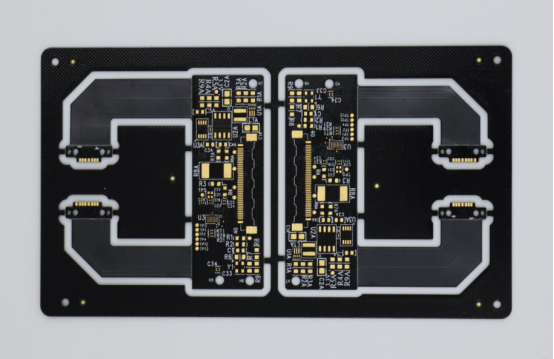
Understanding PCB Laser Hole Drilling: Comparing UV, CO₂, and Ultrafast Lasers
Laser drilling in PCB manufacturing is at the forefront of precision engineering, transforming how we create the tiny, intricate holes that are essential for modern electronics. As electronic devices become more compact and complex, the demand for higher precision in PCB fabrication has led to the adoption of advanced laser technologies. From the sharp, clean cuts of UV nanosecond lasers to the rapid, efficient power of CO₂ lasers and the cutting-edge precision of ultrafast lasers, each method brings unique advantages and challenges. Understanding the differences in these technologies is key to choosing the right one for specific PCB applications, whether it’s achieving micro-scale holes or optimizing production efficiency. In this article, we’ll explore how each laser technology works, their strengths and limitations, and how they are revolutionizing PCB hole drilling.
How Does UV Nanosecond Laser Create Precise Holes in PCBs?
UV nanosecond lasers operate by emitting ultraviolet (UV) light with a wavelength of 355nm. UV light has a high photon energy, making it highly absorbable by most materials, especially those like resins and copper used in PCBs. The laser pulse duration is in the nanosecond range (10⁻⁹ seconds), meaning the laser beam delivers a very short burst of intense energy.
The process begins with photo-chemical ablation, where the UV light interacts with the material at the atomic level. This energy excites electrons, causing them to move rapidly, which leads to material vaporization. Unlike traditional heat-based methods, UV nanosecond lasers cause minimal heat buildup. The material essentially boils off rather than melting, which is why this process is so precise. The result is a clean hole with minimal thermal distortion.
Advantages of UV Nanosecond Laser in PCB Hole Processing
One of the primary advantages of using UV nanosecond lasers for PCB hole drilling is their high precision. This laser type allows for micro-hole drilling with exceptional accuracy, making it ideal for applications like microelectronics where tiny, fine holes are required.
Another key benefit is high processing efficiency. Despite its precision, UV nanosecond lasers can quickly drill through materials without significant delays. This makes them suitable for both high-volume production and more intricate designs.
Additionally, the laser's minimal thermal impact is a major advantage in PCB production. The laser's short pulse minimizes heat diffusion, reducing the thermal impact zone and preventing the surrounding material from suffering damage. This makes UV lasers ideal for fine-tuned, delicate components where heat could affect performance, such as high-frequency circuits.
Disadvantages and Challenges of UV Nanosecond Lasers
While UV nanosecond lasers are an excellent choice for precision, they do have some drawbacks. One of the common issues is the residual material left behind in the form of micro slag or recast layers. This happens because of the intense, focused energy in such short bursts, which can cause some material to re-solidify on the hole's edges. These remnants might not be significant but can affect the quality of the hole and require additional cleaning steps.
Another challenge is minor carbonization that can occur at the edges of the holes. While the laser doesn’t produce significant heat, the energy can still lead to some minor burning of organic materials, leaving a light carbonized layer on the hole's surface. This is generally less severe than with longer laser pulses but still requires attention to detail, especially in the production of high-precision boards.
How Does CO₂ Laser Process Holes in PCBs?
CO₂ lasers use a 9400nm wavelength, which falls in the infrared spectrum. This wavelength is highly absorbable by non-metallic materials such as organic compounds, resins, and plastics commonly used in PCBs. However, it is not absorbed by metals, which is why additional treatments like copper layer removal are required before using CO₂ lasers on PCBs.
The laser operates using a thermal ablation mechanism. When the infrared light hits the material, it transfers energy to the material, causing the surface to heat up gradually. The material absorbs the energy and starts to vaporize once it reaches its boiling point. This means the CO₂ laser works by heating the material continuously until it reaches the temperature necessary to vaporize and remove it. The process generates significant heat transfer, which can affect surrounding areas of the material, making it less suitable for precise, small-scale drilling compared to other laser types.
Advantages of CO₂ Laser in PCB Hole Processing
CO₂ lasers have a few notable advantages when it comes to PCB hole processing:
High Speed for Non-Metal Materials: CO₂ lasers are particularly efficient for drilling holes in non-metallic materials. The high absorption rate of infrared light allows for faster hole formation, making them ideal for large-scale production of PCBs with materials like fiberglass or resin-based boards.
Cost-Effective: Compared to more advanced lasers like UV or ultrafast lasers, CO₂ lasers are generally less expensive. Their relatively low operating and maintenance costs make them a popular choice for mass production of PCBs, particularly in industries where cost efficiency is important.
Perfect for Through-Hole and Blind Hole Expansion: CO₂ lasers excel in through-hole drilling and blind hole expansion, processes where speed is often more important than extreme precision. These lasers can rapidly and effectively cut through the board without excessive concern for precision in smaller holes.
Disadvantages and Limitations of CO₂ Lasers
While CO₂ lasers are efficient and cost-effective, they do have several limitations that can affect the quality of the final product:
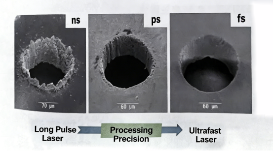
Large Heat-Affected Zone and Rough Hole Walls: The continuous heat application during the drilling process leads to a larger heat-affected zone (HAZ) around the hole. This can result in rougher hole walls and an overall less clean hole compared to lasers with smaller heat zones, like UV nanosecond lasers.
Carbonization and Residual Slag: Due to the high temperatures, carbonization of the material's surface can occur, especially in organic materials like resins. Additionally, the vaporized material can leave behind slag or molten residues around the hole, which might need cleaning or further processing.
Lower Precision for Small Holes: CO₂ lasers are more suitable for larger holes (typically >50μm). When it comes to very small hole sizes and high precision requirements, other laser types (such as UV or ultrafast lasers) tend to perform better.
How Does Ultrafast Laser Achieve High-Precision Hole Processing in PCBs?
Ultrafast lasers operate using extremely high peak power in a very short pulse duration (femtoseconds or picoseconds). This allows the laser to interact with the material in a unique way, called "cold processing." In this process, the laser energy is absorbed by the material’s electrons almost instantaneously. These electrons become highly energized and vaporize the material directly, without transferring the energy to the surrounding atoms (the lattice structure). This means there is minimal thermal impact on the surrounding material.
The main advantage of this process is non-thermal ablation—the material is removed in a solid state without melting or burning. Because the pulse duration is so short, there is no time for heat to spread, which minimizes the heat-affected zone (HAZ), making ultrafast lasers ideal for precision drilling in PCBs. The extremely rapid pulses effectively evaporate the material without causing significant heat damage to nearby areas.
Advantages of Ultrafast Lasers in PCB Hole Processing
Minimal Heat-Affected Zone (HAZ): Since ultrafast lasers don’t rely on heat diffusion, they produce almost no thermal damage to the surrounding material. This results in smooth hole walls and sharp edges without the risk of heat-induced distortion, a crucial factor in the high-precision fabrication of PCBs.
No Slag, No Microcracks: Another significant benefit is that ultrafast lasers don’t leave behind molten residues (slag) or microcracks around the holes. The material is vaporized cleanly, ensuring that the hole's surface is perfectly smooth and free of imperfections. This is especially important in applications where high-frequency signals or sensitive components are involved, as imperfections can interfere with performance.
Capable of Processing Hard and Brittle Materials: Ultrafast lasers excel at machining materials that are typically difficult to process, such as high-hardness or brittle materials. This includes certain ceramics, glass, and even highly reflective metals like gold and copper, which are typically challenging for conventional lasers to handle.
Disadvantages and Challenges of Ultrafast Lasers
High Cost and Complex Technology: The most significant challenge with ultrafast lasers is their high cost. Both the equipment and the operating costs are significantly higher compared to other laser technologies. Additionally, the complexity of the technology requires specialized knowledge and skilled operators, making it less accessible for smaller-scale or low-budget operations.
Slower Processing Speed: Due to the high precision involved in each pulse, ultrafast lasers tend to be slower than other laser types like CO₂ lasers or UV nanosecond lasers, which are faster in terms of material removal. Ultrafast lasers are ideal for tasks where extreme precision is needed, but they may not be the best option for high-volume production where speed is a priority.
How to Choose the Right Laser Technology for PCB Hole Processing?
When selecting the right laser technology for PCB hole processing, it’s essential to consider factors like material compatibility, precision requirements, and production volume. Each laser type—UV nanosecond, CO₂, and ultrafast lasers—offers unique benefits and limitations that make them suitable for different applications.
| Laser Type | Wavelength | Processing Mechanism | Advantages | Disadvantages | Best For |
| UV Nanosecond Laser | 355nm (Ultraviolet) | Photo-chemical ablation, minimal hea | - High precision - Minimal thermal impact - Efficient for micro-hole drilling | - Micro slag or recast layers - Minor carbonization | Microelectronics, high-precision small holes |
| CO₂ Laser | 9400nm (Infrared) | Thermal ablation | - Fast processing for non-metals - Cost-effective - Suitable for large holes | - Large heat-affected zone - Carbonization and slag - Lower precision for small holes | High-volume production, larger holes, through-hole drilling |
| Ultrafast Laser | Femtosecond/Picosecond | Cold processing, non-thermal ablation | - Extremely high precision - No slag or microcracks - Can process hard, brittle materials | - High cost - Slow processing speed - Complex technology | High-precision tasks, hard materials, delicate components |
With various laser types available—each offering unique advantages and limitations—it's important to match the technology to your specific material, hole size, and production requirements. Whether you're focusing on high-precision micro-hole drilling or cost-effective mass production, understanding how to select the best laser based on these factors will help you achieve the desired results while managing costs.
Choosing the Right Laser Based on Material Type
When selecting a laser for PCB drilling, the material being processed plays a crucial role. Different materials require specific laser types for optimal performance.
Resins and Plastics: UV nanosecond lasers are ideal for drilling micro-holes in materials like resins and plastics because their high photon energy allows them to easily penetrate and vaporize these materials without excessive heat. This minimizes thermal damage and results in clean holes.
Copper: UV lasers are also effective for drilling copper layers in PCBs, but CO₂ lasers may be preferred when working with thicker layers. However, CO₂ lasers can leave rough edges due to their larger heat-affected zones, making UV lasers a better choice for precision.
Ceramics and Hard Materials: Ultrafast lasers are best suited for drilling hard or brittle materials, such as ceramics. These lasers have minimal heat impact and can process materials that other lasers struggle with, achieving high precision without cracking or thermal damage.
The thermal sensitivity of the material directly influences which laser technology will work best. For materials that are heat-sensitive, lasers with shorter pulses (like UV or ultrafast lasers) are preferable to minimize thermal damage.
Choosing the Right Laser Based on Hole Size and Precision Requirements
When deciding on a laser, it's important to consider the size of the holes you need to create and the level of precision required.
Small Holes (Micron Range): If your PCB requires micro-hole drilling, UV nanosecond lasers or ultrafast lasers are the best options. These lasers can produce holes with diameters as small as 10 microns, making them suitable for high-precision applications such as microelectronics and fine pitch circuits.
Larger Holes: For larger holes (greater than 50 microns), CO₂ lasers are more suitable. They are faster and more efficient for drilling larger holes but lack the precision required for smaller diameters. CO₂ lasers are commonly used for through-hole drilling and blind hole expansion in non-metallic materials like fiberglass.
Each laser technology has its strengths based on the desired hole size and precision. Ultrafast lasers are ideal for precision-focused tasks, while CO₂ lasers handle larger, quicker tasks more effectively.
Choosing the Right Laser Based on Production Cost and Efficiency
The choice of laser technology should also factor in production cost and efficiency based on the scale of manufacturing.
Small-Batch Production: For small-batch or custom PCB production, ultrafast lasers are the best choice. They provide unmatched precision and can handle complex designs with minimal thermal impact. However, they come at a higher cost, both in terms of equipment and operational expenses.
Large-Scale Production: If you are looking at high-volume production, CO₂ lasers offer the best balance of cost-effectiveness and speed. Their lower initial investment and operational costs make them ideal for manufacturing standard PCBs where precision is less critical.
Return on Investment (ROI) is also a key consideration. While ultrafast lasers offer excellent quality, their high costs make them less suitable for mass production unless extreme precision is required. In contrast, CO₂ lasers provide a good ROI for larger production runs due to their lower cost and high efficiency, despite sacrificing some precision.
Conclusion
Selecting the right laser technology for PCB hole processing depends on a variety of factors, including material type, hole size, precision, and production volume. Whether you prioritize speed, precision, or cost-effectiveness, there’s a laser solution that can meet your specific needs. For manufacturers looking to ensure high-quality results, partnering with an experienced supplier can make all the difference. With years of expertise in advanced PCB manufacturing, PCBMASTER provides tailored solutions that leverage the latest laser technologies to meet the demands of even the most complex projects. Whether you’re in need of high-precision drilling or mass production efficiency, PCBMASTER ensures that your PCBs are crafted to the highest standards.
FAQs
Does UV Nanosecond Laser Processing Leave Slag on Hole Walls?
Yes, although UV nanosecond lasers produce a relatively small heat-affected zone, there can still be small amounts of slag or recast layers left behind on the hole walls. This is due to the intense energy of the laser pulse, which can cause some material to re-solidify at the edges of the hole. While this effect is minimal compared to longer pulse lasers, it may still require additional cleaning or post-processing to ensure optimal hole quality.
What is the Main Difference Between CO₂ Laser and UV Nanosecond Laser?
The primary difference between CO₂ lasers and UV nanosecond lasers lies in their material compatibility, hole size, and processing speed:
| Laser Type | Material Compatibility | Hole Size | Processing Speed | Heat-Affected Zone | Applications |
| CO₂ Laser | Non-metallic materials like fiberglass, ceramics, plastics | Larger holes (typically >50μm) | Fast | Larger heat-affected zone | High-volume production, through-hole drilling, larger hole sizes |
| UV Nanosecond Laser | Materials like resins, copper, plastics | Small-diameter holes (e.g., microelectronics) | Slower | Minimal heat impact | High-precision hole drilling, microelectronics, fine-pitch circuits |
What Are the High-End PCB Processing Needs That Ultrafast Lasers Are Suitable For?
Ultrafast lasers are primarily used for high-precision and micro-hole drilling applications, especially when extremely small hole diameters and sharp, clean edges are required. These lasers are particularly beneficial for advanced PCB manufacturing in industries such as high-frequency electronics, medical devices, and optical components, where the smallest holes, minimal thermal damage, and no cracking are critical. Their ability to process hard, brittle, and reflective materials also makes them suitable for cutting-edge applications that demand the highest level of accuracy and precision.
How Can You Reduce the Heat-Affected Zone in Laser Processing?
To reduce the heat-affected zone (HAZ) and maintain higher processing precision, it is advisable to choose ultrafast lasers or UV nanosecond lasers. Both of these laser types feature extremely short pulse durations, which means the energy is applied in such a short amount of time that there is very little opportunity for heat to spread to surrounding areas. As a result, they can minimize thermal damage to the material and ensure that the surrounding areas are not affected. These lasers are ideal for tasks that require high precision and where even minimal heat damage would affect the integrity of the PCB.
How to Address Slag Issues When Using CO₂ Lasers for PCB Processing?
When using CO₂ lasers to process PCBs, slag or molten residue can sometimes accumulate around the edges of holes due to the heat and vaporization process. To minimize this issue, there are a few steps you can take:
Remove the Copper Layer: One effective method is to remove the copper layer from the PCB's surface before applying the CO₂ laser. This can be done using a chemical or mechanical process to expose the underlying material, such as resin. Once the copper layer is removed, CO₂ lasers can cut more cleanly and with less risk of slag formation.
Control Copper Foil Thickness: Another solution is to control the copper foil thickness to around 9μm or less, ensuring the laser can penetrate through the copper without excessive heating. This helps prevent the material from becoming molten and forming residues around the hole edges.
By taking these precautions, you can reduce slag formation and improve the overall quality of the hole during CO₂ laser processing.
Author Bio
Hi, I'm Carol, the Overseas Marketing Manager at PCBMASTER, where I focus on expanding international markets and researching PCB and PCBA solutions. Since 2020, I've been deeply involved in helping our company collaborate with global clients, addressing their technical and production needs in the PCB and PCBA sectors. Over these years, I've gained extensive experience and developed a deeper understanding of industry trends, challenges, and technological innovations.
Outside of work, I'm passionate about writing and enjoy sharing industry insights, market developments, and practical tips through my blog. I hope my posts can help you better understand the PCB and PCBA industries and maybe even offer some valuable takeaways. Of course, if you have any thoughts or questions, feel free to leave a comment below—I'd love to hear from you and discuss further!

