


Understanding Impedance: Essential Concepts for Electronics and PCB Design
Impedance is a fundamental concept in electrical engineering, yet many overlook its crucial role in modern electronics. Unlike simple resistance, impedance encompasses not just a conductor's opposition to current, but also its interaction with alternating signals, involving resistance, capacitive reactance, and inductive reactance. As electronic devices grow more complex and signals faster, understanding and managing impedance becomes essential for ensuring signal integrity, power efficiency, and electromagnetic compatibility. Whether designing high-speed PCBs, audio systems, or wireless communication circuits, impedance control is key to optimizing performance and minimizing issues like signal reflection and distortion. This article dives into the basics of impedance, exploring its types, influencing factors, and real-world applications—providing you with the knowledge to improve your designs and avoid common pitfalls.
What is Impedance?
Definition and Concept of Impedance
Impedance is the total resistance that a circuit offers to the flow of alternating current (AC). Unlike simple direct current (DC) resistance, which only measures the opposition to current in a steady state, impedance also takes into account the effects of frequency and the properties of the materials in the circuit. It is represented by the symbol Z and combines three key elements:
l Resistance (R) – The opposition to current flow due to the material properties of the conductor, like copper or aluminum. This is the same as DC resistance.
l Capacitive Reactance (Xc) – The opposition caused by capacitors in the circuit. It depends on the frequency; higher frequencies cause less opposition (lower reactance).
l Inductive Reactance (Xl) – The opposition caused by inductors in the circuit. It increases as the frequency goes up.
In simple terms, impedance is like the "total resistance" but for AC circuits, considering both resistive and reactive effects.
The Role of Impedance in Circuits
Impedance plays a critical role in how voltage and current interact in AC circuits. It determines how much current flows for a given voltage, affecting both the magnitude and phase of the signals. Here's how impedance influences circuits:
l Current and Voltage Relationship: Impedance controls how current flows through a circuit when an AC voltage is applied. Ohm's Law still applies, but instead of just resistance, impedance takes into account both resistive and reactive components. This means that even if a circuit has resistance, the current's behavior changes based on the frequency of the applied AC signal.
l Signal Transmission: Impedance mismatch in circuits can lead to reflections of the signal, causing interference and distorted waveforms. This is especially crucial in high-speed communication systems or digital circuits where signal integrity is essential. For example, a mismatch in the impedance of a transmission line can result in signal reflections that corrupt the data.
l Energy Transmission Efficiency: When the impedance of the source, transmission line, and load match, the maximum amount of power is transferred with minimal loss. If the impedances are mismatched, some energy is reflected back to the source, reducing the efficiency of the system. In practical terms, think of it like trying to pour water through a pipe that is too small or too large—most of the water won’t make it to the end.
Why Is Impedance Crucial in Electronic Design?
Impedance is crucial in electronic design because it ensures efficient signal transmission, prevents distortion, and minimizes energy loss and electromagnetic interference.
Signal Integrity and Impedance Matching
Why is impedance matching important for signal integrity?
Impedance matching is essential for ensuring that signals travel through a circuit without distortion or loss. When the impedance of the transmission line (like a PCB trace or cable) doesn't match the impedance of the source or load, signal reflections can occur. These reflections cause parts of the signal to bounce back toward the source, leading to interference and data errors.
How does impedance mismatch affect signal waveforms?
When impedance is not matched, you may see issues like overshoot and undershoot in the signal waveform. For example, overshoot occurs when the voltage spikes higher than the expected value, while undershoot happens when the voltage falls below the normal value. These disruptions can distort the signal, making it harder for the receiver to correctly interpret the data. Over time, this can lead to unreliable system performance, especially in high-speed digital circuits like USB, HDMI, or DDR memory.
In simple terms, think of it like sending water through pipes of different sizes—some of the water will leak back, disrupting the flow. Matching the size of the pipes (impedance) ensures smooth, uninterrupted water flow (signal transmission).
Energy Transmission Efficiency and Impedance Matching
How does impedance matching help achieve maximum energy transfer?
Impedance matching ensures that the energy from the signal source is efficiently delivered to the load without loss. If the impedances of the source, transmission line, and load are not the same, some of the energy is reflected back, reducing the total power transferred. This is similar to trying to push a ball through a narrow pipe—if the pipe is too big or too small, some of the force will be wasted, and the ball won't make it to the other side.
For example, in RF (radio frequency) systems, such as antennas or communication equipment, impedance matching is crucial to minimize signal loss and ensure efficient power transfer. Without proper matching, power is wasted, and the signal strength decreases.
What is the “perfect road” for energy transfer?
The "perfect road" for energy transfer is a scenario where the impedance of all components—source, transmission line, and load—are matched. This is like a smooth, continuous pipe where water flows freely without resistance. By ensuring this match, energy is transmitted with minimal loss, and the system operates efficiently.
Electromagnetic Compatibility (EMC) and Impedance
How does impedance mismatch cause electromagnetic interference (EMI)?
When there’s impedance mismatch in a circuit, part of the signal energy is reflected, and this can radiate as electromagnetic interference (EMI). This unwanted radiation can disrupt nearby electronic devices, causing malfunctions or performance degradation. For instance, in high-frequency circuits like Wi-Fi routers, if impedance isn't matched properly, the reflected energy can leak into the air, interfering with other wireless devices.
How does proper impedance matching reduce electromagnetic radiation?
By ensuring that impedance is matched, the reflected energy is minimized, which reduces EMI. When the impedance is properly controlled, signals flow smoothly, and less energy is radiated as unwanted noise. This is especially critical in sensitive systems like medical equipment, smartphones, or military communications, where even minor interference can cause major issues.
In simple terms, think of impedance matching like sealing a pipe to prevent leaks. With a well-sealed system, no unwanted energy escapes, leading to better performance and fewer disruptions. Proper impedance matching is a fundamental step in achieving electromagnetic compatibility (EMC) and ensuring your device operates smoothly in a noisy electronic environment.
What Are the Types of Impedance?
The main types of impedance are characteristic impedance (including microstrip and stripline) and differential impedance, each suited for different signal transmission needs and applications.
Characteristic Impedance and Single-Line Impedance
What is characteristic impedance, and how does it differ from single-line impedance?
Characteristic impedance refers to the impedance a signal experiences as it travels along a transmission line, such as a PCB trace or a coaxial cable. This type of impedance is constant along the line and depends on factors like the line's width, the material it’s made from, and its surroundings. Single-line impedance usually refers to the impedance of a single trace or wire in isolation, considering factors like its length and the conductor material.
Microstrip vs. Stripline: Key Differences
l Microstrip: A type of transmission line found on the outer layers of a PCB, typically having only one reference plane, like a ground plane on an inner layer. Microstrips are easier to design but more susceptible to environmental influences, such as temperature and humidity.
l Stripline: A transmission line buried within a PCB, sandwiched between two reference planes (ground layers), providing better shielding and less susceptibility to external interference. However, it is harder to manufacture and requires precise control over the PCB layers.
Applications of Different Transmission Lines
l DDR (Double Data Rate): Often uses microstrip lines due to their high-speed requirements and relatively simple manufacturing processes.
l HDMI (High Definition Multimedia Interface): Also uses microstrip or stripline configurations to maintain high-frequency signal integrity.
l USB (Universal Serial Bus): Typically employs microstrips on the PCB to balance cost and performance for fast data transfer.
Comparison Table: Microstrip vs. Stripline
| Feature | Microstrip | Stripline |
| Location | Outer layer of PCB | Sandwiched between layers |
| Shielding | Less shielded, exposed to external factors | Better shielded, less interference |
| Manufacturing | Easier to design and manufacture | More complex design and manufacturing |
| Common Uses | High-speed data (DDR, USB) | High-frequency RF signals (e.g., Wi-Fi) |
Differential Impedance and Two-Line Impedance
What is differential impedance, and why is it important?
Differential impedance refers to the impedance between two conductors that carry opposite, or differential, signals. The two conductors are tightly coupled, meaning they affect each other’s electromagnetic fields, which makes them ideal for high-speed signaling. This type of impedance is particularly important because it provides better noise immunity and reduces electromagnetic interference (EMI).
How do differential signals work, and what are their advantages?
Differential signals carry information as two complementary signals (positive and negative). When both signals are transmitted, any external noise that affects both lines equally will be canceled out when the receiver reads the difference between the two signals. This results in a cleaner signal and lower noise levels, making differential signaling ideal for high-speed, noise-sensitive applications. Examples include USB, PCIe, and SATA connections.
Common Applications for Differential Impedance
l USB (Universal Serial Bus): Uses differential signaling for fast data transfer while minimizing noise, enabling higher data rates and better overall performance.
l PCIe (Peripheral Component Interconnect Express): Relies on differential signaling for high-speed communication between computer components, such as CPUs and GPUs.
l SATA (Serial ATA): Uses differential impedance to transmit data between storage devices, ensuring reliable and fast data transfer.
Comparison Table: Differential Impedance vs. Single-Line Impedance
| Feature | Differential Impedance | Single-Line Impedance |
| Signal Type | Two complementary signals (positive & negative) | Single signal |
| Noise Immunity | Higher immunity, noise cancellation | Lower immunity, susceptible to noise |
| Common Uses | USB, PCIe, SATA, Ethernet | General signal lines, low-speed circuits |
| Signal Integrity | Better for high-speed, long-distance transmission | Good for low-speed, short-distance transmission |
What Factors Affect Impedance?
Impedance is affected by factors such as line width, dielectric thickness, dielectric constant (Dk), copper foil thickness, soldermask ink, and the spacing between differential signal traces.
The Relationship Between Line Width and Impedance
How does line width affect impedance?
Line width plays a significant role in determining the impedance of a transmission line. The wider the line, the lower the impedance. This is because a wider line increases the surface area, allowing for more current to flow, thus reducing the resistance and impedance. Conversely, a narrower line results in higher impedance.
In practical terms, if you are designing a PCB and need to reduce impedance, you would increase the width of the signal trace. For example, in high-speed digital circuits, carefully adjusting the line width can help match the impedance to other circuit components, ensuring smooth signal transmission with minimal reflection.
The Effect of Dielectric Thickness on Impedance
How does the thickness of the dielectric layer affect impedance?
The dielectric thickness—the distance between the signal trace and the ground plane—directly impacts the impedance. As the dielectric layer becomes thicker, the impedance increases. This happens because a thicker dielectric reduces the coupling between the signal trace and the reference plane, which leads to higher resistance to the flow of the signal.
Choosing the right dielectric thickness is essential for controlling impedance, especially in high-frequency circuits. For example, in RF (radio frequency) designs, where signal integrity is crucial, selecting the proper thickness helps maintain the desired impedance to avoid signal loss and distortion.
How does the choice of insulation material affect impedance?
The choice of insulating material between the trace and ground plane (such as FR-4, PTFE, or polyimide) also impacts impedance. Materials with different dielectric constants (Dk) will change how signals interact with the transmission line. A material with a higher Dk will increase the impedance, while a lower Dk material will decrease it.
Dielectric Constant (Dk) and Impedance
How does the dielectric constant (Dk) affect impedance?
The dielectric constant (Dk) is a property of the insulation material that affects how easily electric fields can pass through it. The higher the Dk, the greater the impedance of the transmission line. This is because materials with a higher Dk store more charge, affecting the signal's speed and impedance.
For instance, FR-4, a common PCB material, has a Dk ranging from 3.8 to 4.5 at standard frequencies. Choosing materials with higher or lower Dk values will directly impact the impedance of the transmission lines, influencing the overall performance of the circuit.
What is the difference between high-Dk and low-Dk materials?
l High-Dk materials: These materials (like ceramics) increase impedance and reduce signal speed, which can be useful in specific applications requiring high impedance, such as in certain RF designs.
l Low-Dk materials: Materials like PTFE or low-loss laminates lower the impedance and can help with faster signal transmission, making them ideal for high-speed digital or high-frequency designs.
The Effect of Copper Foil Thickness on Impedance
How does copper foil thickness affect impedance?
Copper foil thickness affects the impedance by altering the overall resistance of the transmission line. Thicker copper foil lowers the resistance and can reduce the impedance. This is because thicker copper allows for more current to flow without as much opposition. In high-frequency designs, copper thickness is crucial for achieving the desired impedance.
Engineers can control impedance in PCB designs by adjusting the copper thickness during the manufacturing process. For example, if you need to lower the impedance in a high-speed digital circuit, increasing the copper foil thickness can help achieve this goal.
The Impact of Soldermask Ink on Impedance
How does soldermask ink affect microstrip impedance?
Soldermask ink, which is applied to the surface of PCBs to protect the copper traces, can also influence the impedance, particularly in microstrip designs. The ink typically has a higher dielectric constant than the copper and can raise the impedance. The thickness and coverage of the soldermask layer can lead to slight variations in impedance, especially for high-frequency signals.
In PCB designs, it's important to ensure the soldermask is evenly applied and within controlled thicknesses to maintain consistent impedance, especially in high-speed or sensitive signal paths.
The Effect of Line Spacing on Differential Impedance
How does the line spacing affect differential impedance?
In differential impedance designs, such as those used for high-speed serial communication (e.g., USB, PCIe), the spacing between the two signal traces is crucial. The closer the lines are to each other, the lower the differential impedance. This is because the signals in the two traces are more strongly coupled, enhancing the signal integrity.
To optimize the differential impedance for specific applications, engineers carefully adjust the trace spacing. For instance, for a typical differential impedance of 100Ω (common in USB and Ethernet), the spacing between the two traces will be optimized based on the PCB material, thickness, and other factors to ensure a smooth, high-quality signal transmission.
Why Is Impedance Important in Practical Applications?
Impedance is important in practical applications because it ensures efficient signal transmission, minimizes distortion, and optimizes power transfer across various systems like audio, RF communication, digital circuits, and power transmission.
Impedance Matching in Audio Systems
How does impedance matching improve audio quality?
Impedance matching is crucial for delivering the best sound quality in audio systems. When the impedance of speakers matches the output impedance of the amplifier, maximum power is transferred from the amplifier to the speakers. This reduces signal loss and distortion, resulting in clearer, more accurate sound. Without proper impedance matching, sound quality may suffer due to poor power transfer or unwanted noise.
Example of impedance matching between speakers and amplifiers
For example, most home audio systems use speakers with an impedance of 8 ohms, while many amplifiers are designed to drive speakers at this impedance. If you connect an 8-ohm speaker to a 4-ohm amplifier, the mismatch will result in inefficient power transfer, potentially causing the system to overheat or distort the audio signal. Ensuring the right impedance match between the amplifier and the speakers maximizes sound clarity and prevents damage.
Impedance Matching in RF and Wireless Communication
Why is impedance matching important between antennas, cables, and transmitters?
In RF (radio frequency) and wireless communication systems, impedance matching ensures that the maximum amount of power is transferred between components like antennas, cables, and transmitters. If impedance is mismatched, some of the signal power will be reflected back, resulting in weaker signals, reduced range, or even malfunction of the communication system.
Application of 50Ω and 75Ω standards
Common impedance values for RF systems include 50Ω and 75Ω. The 50Ω standard is widely used for signal transmission in high-power and high-frequency applications (like antennas and RF test equipment), while 75Ω is typically used for video signals and lower-power applications (such as TV cables). Matching the impedance of these components ensures optimal performance and prevents signal degradation.
Impedance Control in High-Speed Digital Circuits
How is impedance controlled in PCB design to ensure signal integrity?
In high-speed digital circuits, controlling impedance is vital for maintaining signal integrity. For example, in a PCB (printed circuit board), engineers carefully design the traces to have specific impedance values (such as 50Ω) that match the source and load impedances. This minimizes signal reflection, prevents data corruption, and ensures clear, sharp signal transitions at high speeds.
Impedance control techniques for high-speed serial buses
For high-speed serial buses, such as USB and PCIe, proper impedance control is critical for transmitting signals with minimal loss and distortion. Techniques like differential pair routing (where two closely spaced traces carry complementary signals) and controlled trace width are commonly used to maintain consistent impedance throughout the PCB layout. This ensures smooth data transfer without errors or jitter.
Impedance Control in Power Transmission
How does impedance affect power transmission efficiency?
Impedance plays a crucial role in the efficiency of power transmission systems. In electrical grids and power lines, matching the impedance between the source, transmission line, and load helps minimize energy loss during transmission. Mismatched impedance can lead to power reflections, which not only reduce efficiency but may also cause equipment damage over time.
Impedance matching in power systems
In power systems, ensuring impedance matching between components is essential for efficient energy transmission. For example, high-voltage transmission lines are designed to have specific impedance values that allow electricity to flow smoothly over long distances with minimal loss. By controlling impedance, power systems can operate at their highest efficiency, ensuring reliable and cost-effective energy delivery.
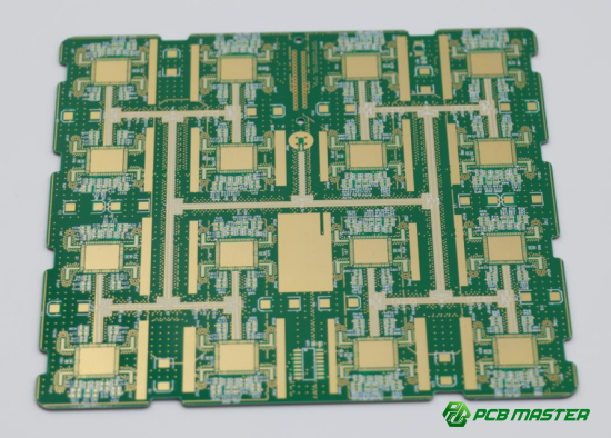
How to Control Impedance in PCB Design?
Impedance in PCB design can be controlled by carefully adjusting trace width, selecting consistent materials, ensuring uniform lamination and etching, and conducting thorough testing with tools like TDR.
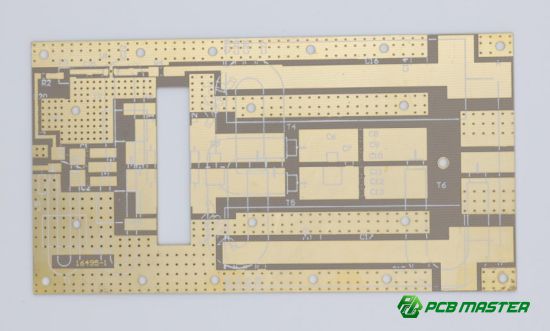
Engineering Processing and Impedance Calculation
How can impedance be adjusted based on customer requirements and process capabilities?
In PCB design, impedance must be calculated and adjusted to meet both the customer's specifications and the manufacturing process's capabilities. Engineers use formulas and simulation tools to calculate the required impedance, considering factors such as line width, material properties, and the dielectric layer thickness. Based on these calculations, adjustments are made to the PCB layout, such as selecting the appropriate trace width or using different materials to ensure the impedance matches the design goals.
For example, a customer may require a 50Ω impedance for high-speed signals like USB or Ethernet. The PCB designer will then adjust trace width and dielectric thickness to meet this requirement, ensuring that the final design supports the desired signal integrity and performance.
How do line width and lamination uniformity affect impedance stability?
The line width and lamination uniformity are critical for maintaining stable impedance. Variations in trace width can lead to fluctuations in impedance, while uneven lamination during the PCB manufacturing process can cause inconsistencies in dielectric thickness. Both factors can result in impedance mismatch, leading to signal degradation and reflection. Engineers must carefully control the manufacturing process to ensure these parameters remain consistent across the board.
Material Consistency and Impedance Control
How do stable substrates and copper foil thickness impact impedance?
The choice of base material (substrate) and copper foil thickness plays a major role in controlling impedance in PCB design. Common PCB substrates like FR4 or Rogers have specific dielectric constants (Dk), which affect how signals propagate along the traces. The copper foil thickness affects the resistance and overall impedance; thicker copper typically lowers the impedance, while thinner copper raises it.
For instance, FR4 has a typical Dk range of 3.8 to 4.5, and using this material, a designer must calculate the correct trace width to achieve the desired impedance. Additionally, consistent copper thickness ensures uniform current distribution across the traces, supporting the overall impedance stability.
How can material consistency be ensured?
To guarantee material consistency, PCB manufacturers must ensure that base materials, copper foil thickness, and other components meet strict quality control standards. Variations between material batches can lead to impedance mismatches and impact the overall performance of the PCB. Regular material testing and sourcing from reliable suppliers help maintain consistency.
Key Impedance Control Points in the Production Process
How do etching uniformity and lamination quality control affect impedance?
In the production process, etching uniformity is crucial for maintaining consistent trace width across the PCB. If the etching process is uneven, the width of the traces will vary, leading to fluctuating impedance. Lamination quality control is equally important because the uniformity of the dielectric layer (the material between the traces and ground) impacts the impedance. Any inconsistencies in the lamination process can lead to variations in impedance along the traces, affecting signal integrity.
For example, in high-frequency circuits, even small changes in trace width or dielectric thickness can cause significant impedance deviations. Therefore, manufacturers must implement strict quality checks during both etching and lamination to ensure that the final PCB meets the required impedance specifications.
How does soldermask thickness and uniformity affect impedance?
The soldermask layer applied to the PCB can also influence impedance, particularly in microstrip lines. Since soldermask material has a higher dielectric constant than the PCB substrate, uneven soldermask thickness or improper application can raise the impedance. Therefore, ensuring consistent soldermask application is critical for maintaining impedance control, especially in high-speed signal paths.
Testing and Validation
How is impedance tested using TDR (Time Domain Reflectometer)?
Impedance testing is crucial to verify that the PCB design meets the required specifications. TDR (Time Domain Reflectometer) is a key tool used for impedance testing. TDR sends a fast pulse through the transmission line and measures the reflection that occurs when there is an impedance mismatch. By analyzing the time it takes for the pulse to return, engineers can determine the impedance at any point along the PCB.
TDR is especially useful for detecting problems like signal reflections, which can occur when impedance is mismatched, leading to data errors or signal loss. This allows designers to pinpoint areas where the impedance deviates from the expected values and make necessary corrections.
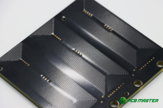
Why are test coupons and test reports important?
Test coupons are specially designed test circuits included in the PCB layout to facilitate impedance testing. These coupons mimic the signal paths of the actual PCB, allowing manufacturers to measure impedance at various points. After testing, a test report is generated that includes detailed information on the measured impedance values, any deviations, and recommendations for corrections. These reports are crucial for verifying that the impedance control was successful and for ensuring the PCB meets the required performance standards.
What Are Common Impedance Testing Methods?
Common impedance testing methods include TDR (Time Domain Reflectometer) testing, which analyzes signal reflections to identify impedance mismatches, and test coupon design, which simulates real PCB conditions to validate impedance accuracy.
TDR Testing and Impedance Validation
What is TDR testing, and how is impedance tested?
TDR (Time Domain Reflectometer) testing is a precise method for measuring impedance along a PCB trace. TDR works by sending a fast electrical pulse down the transmission line. When this pulse encounters any impedance mismatch, part of the pulse is reflected back. The time it takes for the reflection to return is measured and analyzed to determine the location and magnitude of any impedance mismatch.
To perform impedance testing with TDR, the device is connected to the PCB at the test points. The TDR sends a signal, and by analyzing the reflection profile, engineers can identify areas where the impedance deviates from the desired value. This is crucial for detecting signal integrity issues, such as reflections that can cause data errors or performance degradation.
In practice, TDR helps ensure that the PCB design meets the required impedance standards for high-speed signal integrity. For example, USB or PCIe circuits often require precise impedance control, and TDR testing ensures these requirements are met during manufacturing.
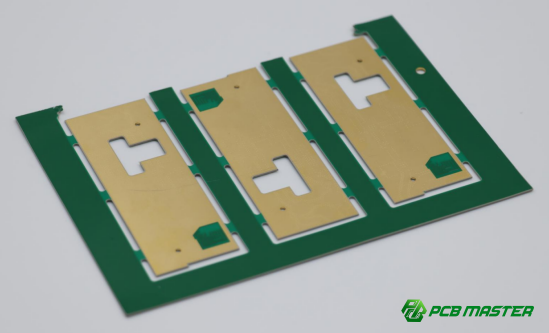
Test Coupon Design and Application
What is a test coupon, and how does it simulate real-world PCB conditions for impedance validation?
A test coupon is a special test circuit designed and added to the PCB layout specifically for impedance testing. It consists of test traces that replicate the actual signal paths on the PCB but are isolated from the primary circuitry. These test coupons allow engineers to measure the impedance of the PCB in a controlled and repeatable way, ensuring that the entire board meets the impedance requirements.
Test coupons are particularly useful for simulating the actual wiring environment of the PCB. By placing test traces next to the primary signal traces, the coupon can account for factors like trace width, dielectric material, and spacing that influence impedance. Engineers use these coupons to perform impedance checks at various stages of production to verify the quality and consistency of the PCB design.
For example, when testing high-speed serial buses like HDMI or DDR, the coupons will be designed to match the exact trace layout, dielectric material, and geometry of the final product, providing reliable impedance measurements. Test coupons ensure that all parts of the PCB are verified for accurate impedance before full-scale production.
Conclusion
Understanding and controlling impedance in PCB design is crucial for ensuring signal integrity, optimal power transfer, and reliable system performance. By employing effective testing methods like TDR and integrating test coupons, engineers can accurately validate impedance throughout the design and manufacturing process. These steps help avoid issues such as signal distortion and data errors, ensuring that your high-speed circuits function as intended.
For businesses looking to guarantee precise impedance control and high-quality PCB designs, partnering with a trusted supplier is essential. That's where PCBMASTER, a trusted PCB and PCBA supplier, comes in. With years of experience in the industry, PCBMASTER offers expert services in impedance management, along with advanced manufacturing capabilities to meet the most demanding design requirements. Whether you're working on high-speed digital circuits or RF applications, PCBMASTER provides reliable solutions that ensure your designs meet the highest standards of performance and reliability.
FAQs
1. What Is the Difference Between Impedance and Resistance?
Impedance and resistance are both measures of opposition to the flow of electrical current, but they behave differently in AC (alternating current) and DC (direct current) circuits.
l Resistance applies to DC circuits and represents the opposition to current flow due to the material and physical properties of a conductor. It is a scalar quantity that does not change with frequency.
l Impedance, on the other hand, applies to AC circuits and takes both the resistance and reactance (which includes capacitive and inductive opposition) into account. Impedance is a complex quantity, meaning it has both magnitude and phase, and it changes with frequency.
While resistance only limits current in DC circuits, impedance can affect both current and voltage in AC circuits, causing phase shifts between them.
2. How to Calculate Impedance in PCB Design?
In PCB design, impedance is calculated based on several factors like trace width, dielectric thickness, and material properties.
l Trace Width: The width of the signal trace influences impedance. Wider traces lower the impedance, while narrower traces raise it. This relationship can be quantified using formulas like the microstrip impedance equation or by using simulation tools.
l Dielectric Thickness: The thickness of the insulating material (the dielectric) between the trace and the ground plane affects impedance. Thicker dielectrics generally result in higher impedance because they reduce the coupling between the trace and the reference plane.
l Material Properties: The dielectric constant (Dk) of the material between the trace and ground also impacts impedance. Materials with higher Dk will generally produce lower impedance.
To accurately calculate and adjust impedance in PCB design, tools like simulation software or online impedance calculators are often used, which factor in the geometry of the trace, the material properties, and the operating frequency.
3. What Problems Does Impedance Mismatch Cause?
Impedance mismatch can lead to several issues in signal integrity:
l Signal Reflection: When the impedance of a PCB trace doesn't match the impedance of the source or load, part of the signal is reflected back to the source, leading to signal loss and delayed signals.
l Distortion: Reflection can distort the signal waveform, causing issues like overshoot, ringing, or undershoot in digital signals. These artifacts can result in data errors or degraded performance in high-speed circuits.
l Reduced Power Transfer: Mismatched impedance can lead to inefficient power transfer, causing a loss in signal strength and energy, which is critical in high-speed or high-frequency applications.
In RF and high-speed digital circuits, impedance mismatch can cause significant signal degradation, making precise impedance control essential for proper functionality.
4. How to Test If a PCB’s Impedance Meets Design Requirements?
To ensure that a PCB’s impedance matches the design specifications, two primary methods are commonly used:
l TDR Testing (Time Domain Reflectometer): TDR testing involves sending a fast electrical pulse down a transmission line and analyzing the time it takes for any reflections to return. This allows engineers to measure the impedance at various points along the PCB. A TDR test identifies any mismatches in impedance, helping to ensure that signal integrity is maintained.
l Test Coupon Design: Test coupons are designed and incorporated into the PCB layout to simulate actual signal paths. These coupons are used to perform impedance measurements during manufacturing. By measuring the impedance in these coupons, manufacturers can verify that the PCB layout adheres to the required impedance specifications before full-scale production.
Both methods help ensure that the PCB will perform as intended without signal issues such as reflections or data corruption.
5. How Does Impedance Control Improve Circuit Electromagnetic Compatibility (EMC)?
Impedance control plays a crucial role in enhancing electromagnetic compatibility (EMC) by reducing unwanted electromagnetic interference (EMI) and radiation.
l Reducing EMI: Impedance mismatch can cause reflections and increased radiated emissions, leading to EMI. By controlling the impedance and ensuring proper matching across the PCB, reflected signals are minimized, reducing the amount of interference that can escape the circuit and affect nearby components or systems.
l Minimizing Electromagnetic Radiation: Proper impedance matching helps reduce crosstalk and ensures that signals propagate cleanly along the PCB. This minimizes unwanted electromagnetic radiation, which is especially important in high-speed digital and RF circuits where stray signals can interfere with other components.
By maintaining precise impedance throughout the PCB, designers can ensure that their circuits meet EMC standards, improving their immunity to external interference and preventing them from emitting harmful electromagnetic radiation.

