


PCB Hole Roughness Causes and Design Optimization Tips for Better Performance
PCB hole roughness is a critical factor that can impact the quality, signal integrity, and reliability of your design. Even slight imperfections on the hole walls can lead to issues during the electroplating process, causing long-term performance degradation. Understanding the causes behind these rough surfaces is the first step in tackling this challenge.
In many cases, roughness arises from a combination of material issues and manufacturing processes, where improper handling during drilling, etching, or cleaning can leave unwanted marks and burrs on the walls. However, the good news is that with the right design choices, many of these problems can be avoided before they even reach the production line.
This article explores the root causes of PCB hole roughness and offers practical design improvements to mitigate these issues from the start. By optimizing material selection, layer design, and manufacturing parameters, engineers can create more reliable and efficient PCB designs that ensure a smoother, higher-quality final product.
Causes of Roughness in PCB Holes
Roughness in PCB holes is caused by factors such as poor material quality, worn drill bits, incorrect drilling parameters, improper etching, and inadequate pre-plating treatments.
PCB Hole Roughness Caused by Material Issues
PCB hole roughness caused by material issues typically results from poor bonding between glass fiber and resin, insufficient resin toughness, or low-quality glass fiber, leading to uneven hole walls.
How Does Copper-Clad Laminate Quality Affect Hole Roughness?
The quality of the copper-clad laminate (CCL) directly impacts the roughness of PCB holes. Poor material properties can cause the hole walls to be uneven, leading to electrical and mechanical issues in the final product.
l Glass Fiber and Resin Bonding Issues: If the resin used in the CCL does not bond well with the glass fiber, it can cause the fibers to separate during the drilling process. This separation creates a rough surface on the hole walls, as the drill bit pulls away the resin and fiber unevenly. This results in an inconsistent and rough hole surface.
l Insufficient Resin Toughness: Some resins are brittle and lack toughness. When drilling, these resins are more likely to crack or shatter, leading to micro-cracks or fragments instead of smooth, clean edges.
l Poor Glass Fiber Quality: If the glass fiber is loosely woven or unevenly distributed, it can easily be pulled out or disturbed during drilling, resulting in a rough hole surface. High-quality CCLs with tightly woven glass fibers are less prone to these issues.
Example: A PCB used in a high-frequency circuit may suffer signal integrity issues if the glass fiber and resin bond is weak, causing inconsistencies that affect the signal path.
Process Issues Leading to PCB Hole Roughness
Process issues leading to PCB hole roughness include worn drill bits, incorrect drilling parameters, improper cover/backing materials, excessive etching, and incomplete pre-plating treatments.
How Does the Drilling Process Contribute to Hole Roughness?
The drilling process plays a significant role in the roughness of PCB holes. Factors such as worn drill bits, incorrect drilling parameters, and improper use of cover or backing materials can all lead to a rough hole wall.
l Worn Drill Bits: As drill bits wear down, they no longer cut material cleanly. Instead of slicing through the PCB material, they tend to grind or tear it, leading to rough, jagged edges around the hole. Worn drill bits are a common cause of uneven hole surfaces.
l Incorrect Drilling Parameters: The speed and feed rate of the drill bit are critical. If the feed rate is too fast, the bit might tear the material instead of cutting it, leading to rough holes. On the other hand, if the speed is too slow, excessive heat from friction can burn the resin, damaging the hole walls.
l Inappropriate Cover and Backing Materials: Cover materials help prevent bit slippage, while backing materials support the PCB during drilling. If these materials are not chosen correctly—too soft or too hard—they can cause instability during drilling, leading to incomplete hole formation or damage to the hole surface.
Example: In high-density interconnect (HDI) boards, precise drilling is essential. A worn drill bit or incorrect feed rate can cause significant surface irregularities, affecting both the board’s electrical and mechanical performance.
How Does the Drilling Debris Removal Process Affect Hole Roughness?
The debris removal process, which includes cleaning out resin and fiber fragments from the drilled holes, can significantly impact the smoothness of the hole wall. If not done properly, these fragments can cause roughness.
l Excessive Etching: After drilling, PCB manufacturers use chemicals like potassium permanganate to remove resin debris and glass fiber fragments. If the chemical solution is too aggressive or used for too long, it can over-etch the hole walls, creating a rough, pitted surface. Over-etching weakens the resin and can cause structural problems in the PCB.
l Resin and Glass Fiber Corrosion: Chemicals designed to clean the hole often corrode the resin or glass fibers. If the process is not controlled carefully, the glass fibers may dissolve unevenly, creating a jagged texture on the hole walls, which results in roughness.
Example: In a PCB used for RF (radio frequency) circuits, the over-etching of holes may cause signal loss, affecting the board’s ability to transmit or receive signals cleanly.
How Do Pre-Plating Treatment Processes Affect Hole Quality?
Pre-plating treatments, like plasma treatment or chemical cleaning, are essential for preparing the PCB for electroplating. If these processes are not properly executed, they can leave behind residues that affect the plating quality and hole smoothness.
l Plasma Treatment: Plasma is often used to clean the hole walls before plating to ensure the metal adheres properly. If this treatment is insufficient or incomplete, any residual debris, such as drilling dust or resin, can remain inside the hole. This residue can lead to poor plating adhesion and uneven hole walls.
l Chemical Cleaning: Chemical cleaners remove contaminants from the hole surface before electroplating. However, if these chemicals are not used correctly or thoroughly rinsed off, they can leave behind traces that interfere with the plating process, leading to irregularities in the hole surface.
Example: In a high-speed digital PCB, inadequate plasma treatment can lead to poor copper adhesion inside the holes, which can result in unreliable electrical connections or even failure of the PCB in its final application.
How to Optimize the Design to Reduce PCB Hole Roughness?
To optimize the design and reduce PCB hole roughness, choose high-quality materials, carefully plan stack-up and hole attributes, manage hole density, ensure precise drilling, and collaborate closely with manufacturers on quality control.
How to Choose the Right PCB Material to Optimize Hole Wall Quality
To optimize hole wall quality, choose high-performance materials like high Tg laminates, low roughness copper foils, and specialty glass fibers such as open-fiber or flat-fiber cloths.
Why is Choosing High-Performance, Low Roughness Materials Crucial for Hole Wall Quality?
High-performance materials with low roughness help reduce PCB hole surface imperfections, ensuring better electrical and mechanical performance.
l High Tg Materials and Low Roughness Copper Foils: High Tg (glass transition temperature) materials are more stable at higher temperatures and less prone to cracking or degradation during the drilling process. These materials ensure better bonding between resin and glass fibers, which leads to smoother hole walls. Additionally, low roughness copper foils minimize roughness and improve the uniformity of electroplating, leading to a higher-quality hole surface.
l “Open-Fiber” and “Flat-Fiber” Cloths: Special glass fiber cloths, such as open-fiber or flat-fiber cloths, offer better consistency in drilling. Open-fiber cloths are woven in a way that reduces the likelihood of glass fibers being pulled out unevenly, while flat-fiber cloths reduce the gaps between fibers, leading to a smoother hole surface. Choosing these types of cloths can significantly lower the chance of roughness caused by uneven fiber distribution.
Example: In high-frequency applications, like telecommunications, using high Tg materials and flat-fiber cloths ensures minimal signal interference due to smoother hole walls, leading to improved signal integrity.
How to Optimize Stack-Up Design and Hole Attribute Definitions
To optimize stack-up design and hole attribute definitions, avoid small angles between glass fibers and hole walls, use offset stack-up designs, and clearly distinguish PTH from NPTH holes in Gerber files.
How Can Stack-Up Design Help Prevent Hole Wall Roughness?
Proper stack-up design helps control the angle at which the drill bit interacts with the fiber, reducing the risk of rough hole walls.
l Avoid Small Angle Between Glass Fiber and Hole Wall: The angle at which glass fibers align relative to the hole can impact the smoothness of the hole wall. When fibers are aligned at small angles (e.g., 0° or 90°), the drill bit cuts cleanly through the fiber bundles. However, at an angle of around 45°, the drill bit has to cut through more fibers at once, causing uneven cutting and rougher surfaces.
l Using Offset Stack-Up Design: In offset stack-up designs, the core material and prepreg layers are rotated slightly (e.g., 45°) relative to the original alignment. This offset reduces the risk of cutting multiple fibers simultaneously at a small angle, improving hole wall smoothness. However, this design is more expensive and usually used in high-performance boards like those for high-speed or RF applications.
Example: In HDI boards, offset stack-up designs can ensure that high-density interconnections have cleaner, more reliable hole walls, which is crucial for ensuring signal integrity in advanced electronics.
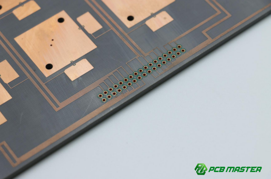
How to Effectively Distinguish PTH and NPTH Holes in Gerber Files?
Properly labeling PTH (Plated Through-Hole) and NPTH (Non-Plated Through-Hole) in Gerber files helps manufacturers apply the right processing steps to each hole type.
l PTH vs. NPTH: PTH holes are meant for electrical connections and need to be plated with copper to conduct signals or power. NPTH holes, on the other hand, are purely mechanical and do not require plating. Clearly distinguishing between these two types in the Gerber files ensures the right manufacturing processes are followed, such as selective etching and plating for PTH holes.
l Clear Labeling: By specifying whether a hole is PTH or NPTH in the design files, manufacturers can apply different cleaning and etching procedures to PTH holes, avoiding unnecessary roughness that could result from over-etching or incorrect processing.
Example: In multi-layer PCBs, failing to distinguish between PTH and NPTH holes may result in unnecessary etching processes on NPTH holes, leading to avoidable roughness in areas where it is not needed.
How to Optimize Drilling Design to Reduce Hole Roughness
To optimize drilling design and reduce hole roughness, manage hole density, ensure uniform hole distribution, carefully design blind and buried holes, and provide accurate hole size and quantity information.
How to Manage Hole Density to Avoid Hole Roughness?
Managing hole density and ensuring uniform hole distribution help reduce drill bit wear and maintain consistent hole quality.
l Hole Density and Drill Bit Wear: High hole density in a small area can lead to increased friction, causing faster drill bit wear. As the drill bit becomes dull, it can create rougher hole surfaces. To avoid this, it’s important to space out holes in high-density areas, reducing the strain on the drill bit.
l Uniform Hole Distribution: Spreading holes evenly across the PCB helps maintain balanced temperature distribution and reduces localized drill bit wear. This results in smoother hole surfaces and extends the lifespan of the drill bits.
Example: In high-density interconnect (HDI) designs, excessive hole density can increase the chances of drill bit wear, leading to rougher hole walls. Proper hole spacing can help avoid this issue and improve the overall quality of the PCB.
What Are the Design Considerations for Blind and Buried Holes?
Blind and buried holes are more difficult to drill and plate, requiring special design considerations to avoid rough hole walls.
l Blind Holes: These are holes that do not go through the entire PCB but connect to other layers. They are harder to drill because the drill bit must be precisely controlled to avoid drilling errors. To ensure smooth hole walls, it’s important to provide clear specifications for hole depth and diameter.
l Buried Holes: These holes are entirely within the layers of the PCB and require even more precision to ensure the drill bit doesn’t cause damage to internal layers. Using the correct drill bit size and maintaining strict control over the drilling process are critical for minimizing roughness.
Example: In advanced multi-layer PCBs used in smartphones, buried and blind holes need to be drilled with extreme precision to avoid any structural weaknesses or surface roughness that could affect functionality.
How to Ensure Accurate Hole Size Information for High-Quality Drilling?
Providing accurate hole size and quantity information in the design files helps manufacturers select the appropriate drill bits and drilling parameters for smoother holes.
l Precise Hole Size and Quantity: Ensuring that each hole’s diameter and quantity are accurately specified in the design files is crucial. Accurate information allows manufacturers to choose the correct drill bit size, reducing the risk of creating rough or inconsistent hole walls.
l Choosing the Right Drill Bit: Different hole sizes require different drill bits. Small holes may require specialized drill bits, while larger holes may need re-sharpened or freshly manufactured bits. Correctly specifying the quantity of each hole size helps the manufacturer optimize tool usage, minimizing wear and ensuring consistent hole quality.
Example: In a complex PCB design for medical devices, small holes with precise tolerances are required to ensure smooth electrical connections. Providing detailed hole specifications ensures that the drilling process is optimized for each hole size, resulting in better hole quality.
How to Collaborate with Manufacturers to Optimize Hole Wall Quality
To collaborate effectively with manufacturers and optimize hole wall quality, clearly specify hole wall requirements in technical files, confirm process capabilities, and verify quality through cross-section reports.
How to Clearly Specify Hole Wall Quality in Technical Files?
Clearly specifying hole wall quality requirements in technical files ensures that manufacturers understand the expected standards and can apply appropriate processes.
l Key Hole Requirements: Marking specific holes in the design files as critical (e.g., for power or high-speed signals) and requiring smooth hole walls without excessive etching can help manufacturers prioritize these areas.
l Smooth Hole Walls and No Over-Etching: Clearly state that the holes should be smooth, free of burrs, and without excessive chemical etching. This will guide the manufacturer’s process control and prevent unnecessary roughness.
Example: For a PCB used in a precision medical instrument, specifying "smooth hole walls" in the technical file ensures that critical holes, such as those used for signal integrity, are manufactured to a high standard.
How to Confirm Manufacturer's Process Capability?
Answer: Confirming a manufacturer’s ability to meet hole wall quality standards before production ensures that the final product will meet design expectations.
l Pre-production and Sampling: Before full-scale production, confirm with the manufacturer that they can meet the hole wall roughness requirements. Request sample boards to verify the quality of drilled holes.
l Process Control Documentation: Request documentation that shows the manufacturer's process controls for drilling, etching, and plating to ensure they align with the desired quality standards.
Example: Before mass production of a new PCB for consumer electronics, conducting a pilot run with the manufacturer ensures that the final product will meet the expected quality standards.
How to Verify Hole Wall Quality Using Cross-Section Reports?
Cross-section reports provide a detailed view of hole wall quality, allowing for verification of smoothness and plating uniformity.
l Cross-Section Reports: These reports offer a close-up view of the drilled holes, showing the wall quality, plating thickness, and any potential imperfections like roughness or uneven plating.
l How to Obtain Reports: Request cross-section analysis during the first batch or periodically during production to monitor the quality of the hole walls. This ensures that any issues are identified early.
Example: In aerospace PCB applications, a cross-section report ensures that holes used for signal transmission are smooth and free of defects, which is critical for high-performance systems.
Conclusion
Ensuring high-quality PCB hole walls begins with a well-thought-out design strategy that addresses key aspects of material selection, stack-up configuration, drilling methods, and clear communication with manufacturers. By choosing the right materials, such as high Tg laminates and low roughness copper foils, and designing with optimal hole density and precise hole size specifications, you can significantly reduce the risk of hole roughness. Additionally, defining the attributes of plated through-holes (PTH) and non-plated through-holes (NPTH) clearly in design files ensures the correct processing steps are followed during manufacturing.
For high-reliability products, such as those used in aerospace, medical, or high-frequency applications, careful attention to every detail of the PCB design is crucial. Ensuring smooth, consistent hole walls not only improves the mechanical strength of the PCB but also enhances signal integrity and long-term durability.
When it comes to ensuring top-notch quality, working with an experienced and reliable PCB manufacturer is essential. Companies like PCBMASTER, with years of expertise in PCB and PCBA manufacturing, are committed to delivering high-quality products that meet stringent industry standards. By leveraging their experience and advanced manufacturing processes, you can rest assured that your PCB designs will be optimized for quality and reliability from start to finish.
FAQs
1. How Does Hole Wall Roughness Affect PCB Performance and Reliability?
Hole wall roughness can significantly impact PCB performance and reliability by causing poor electrical conductivity, signal integrity issues, and weak mechanical strength. Irregular hole surfaces may lead to inconsistent electroplating, which can result in unreliable electrical connections and potential failures, especially in high-frequency or high-reliability applications. Additionally, rough holes can lead to the accumulation of stress at specific points, which may cause cracks or breakage during thermal cycling or mechanical stress.
2. How to Choose the Right PCB Material to Reduce Hole Roughness?
To reduce hole roughness, choose high-quality PCB materials such as high Tg laminates and low roughness copper foils. High Tg materials offer better thermal stability and resistance to cracking, ensuring that the hole walls remain smooth during drilling. Additionally, using specialty glass fibers like flat-fiber or open-fiber cloths can prevent uneven fiber pull-out, which contributes to smoother hole walls. These materials minimize roughness during the drilling and etching process, resulting in higher quality and more reliable PCBs.
3. How to Optimize Hole Layout and Hole Size During Design?
Optimizing hole layout and size during the design phase is crucial to reducing hole roughness. Avoid designing high hole density in small areas, as this can lead to increased wear on the drill bit and uneven hole walls. Instead, distribute holes evenly across the PCB to prevent localized drill bit wear. Additionally, ensure that hole sizes are accurately specified and avoid unnecessary small holes that can lead to drilling difficulties and roughness. Properly optimized hole layouts contribute to a smoother drilling process and more reliable final product.
4. Why Does Drill Bit Wear Cause Hole Wall Roughness?
Drill bit wear contributes to hole wall roughness because a worn drill bit is less effective at cutting through the PCB material cleanly. Instead of producing smooth edges, a dull bit may grind or tear the material, leading to uneven surfaces. Over time, as the drill bit becomes worn, it loses its sharpness, increasing friction and heat, which can cause damage to the hole walls, including cracking, burning, or excessive material removal. Regularly replacing or sharpening drill bits is essential to maintain smooth hole walls.
5. What Manufacturing Details Should Be Focused on When Communicating with PCB Manufacturers?
When communicating with PCB manufacturers, it is essential to clearly specify the hole wall quality requirements in technical documents, especially for critical holes that will carry high-speed signals or power. Ensure that the manufacturer is aware of specific needs, such as smooth hole walls without excessive etching or burrs. Additionally, confirm the manufacturer's ability to handle particular materials, hole sizes, and drilling techniques, especially for complex designs like HDI or multi-layer boards. Regular communication and quality checks, such as requesting micro-section reports, can help ensure that the final product meets the desired specifications.

