


Laser Drilling DFM for PCB Microvias: Design and Manufacturing Best Practices
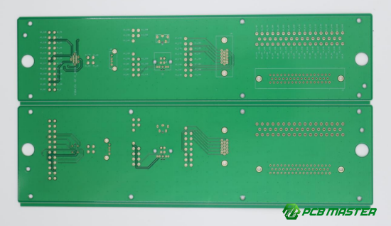
High-density interconnect (HDI) boards rely heavily on the precision and reliability of microvias, where even minor deviations can lead to plating defects, irregular hole shapes, or overall performance issues. At PCBMASTER, years of hands-on PCB manufacturing experience have shown us that optimizing laser drilling during the design-for-manufacturing (DFM) stage is critical to achieving consistent quality.
This guide shares practical insights into laser drilling for microvias, covering material selection, via layout strategies, and production considerations. Engineers and designers will find actionable recommendations to prevent common risks early, ensuring that every PCB not only meets design specifications but also performs reliably throughout its lifecycle.
What is the key role of laser drilling (CO₂ and UV) in PCB microvias?
Laser drilling is a precise method used to create microvias in PCBs, enabling high-density interconnects (HDI) by removing small areas of dielectric material without mechanical stress.
Laser drilling overview and definition of microvias
Laser drilling uses a focused laser beam to remove small sections of PCB material to create holes. A microvia is a very small hole, usually less than 150μm (6 mils) in diameter, that connects one layer of a PCB to another. Unlike mechanical drilling, laser drilling can create tiny, precise holes without causing cracks or delamination.
Example: In a 6-layer HDI board, laser-drilled microvias can connect the top signal layer to an internal power layer in a fraction of a millimeter. This allows more circuits in a smaller board footprint and avoids bulky through-holes.
CO₂ vs. UV lasers: wavelength differences and suitable materials
CO₂ and UV lasers differ in wavelength, which affects how well they drill different PCB materials.
l CO₂ lasers: wavelength ~10.6 μm, ideal for standard epoxy and FR-4 resins because these materials absorb infrared energy efficiently. Glass fibers are harder to remove with CO₂ lasers, sometimes causing irregular holes.
l UV lasers: wavelength ~355 nm, much shorter, can cut through resin and partially through copper, making them suitable for very fine microvias and multilayer boards with dense features.
Comparison example: If a board uses standard FR-4, a CO₂ laser works well. For a high-resolution HDI board with thin resin and copper layers, a UV laser ensures cleaner microvias with less thermal damage.
Microvias in high-density interconnect (HDI) boards: application value
Microvias are essential for HDI boards because they allow more connections in a smaller area, improving performance and reducing board size.
They enable stacked and staggered connections without enlarging the board.
Microvias reduce signal interference because shorter vertical connections reduce inductance and capacitance.
Using laser-drilled microvias also supports multi-layer HDI designs, common in smartphones, laptops, and compact electronics.
Real-life example: A smartphone motherboard with a 0.2mm pitch uses microvias to connect power and signal layers efficiently. Mechanical drilling would be impossible at this density.
How does material selection affect laser drilling performance?
The choice of PCB materials directly affects laser absorption, hole quality, and production yield. Different dielectric materials, glass fabrics, and copper layers interact with CO₂ and UV lasers differently, influencing drilling efficiency and microvia reliability.
Dielectric material absorption characteristics
Dielectric materials’ ability to absorb laser energy determines how clean and efficient the microvia drilling will be.
l FR-4 vs. modified epoxy resins: Standard FR-4 absorbs CO₂ laser energy well, producing clean holes in most boards. Modified epoxy resins, such as Panasonic M-series, may require slightly different laser power due to variations in resin composition. Choosing the right resin ensures consistent hole depth and shape.
l PPO/PPE materials under CO₂ laser: PPO/PPE resins, such as the Taiyo TUC series, absorb CO₂ laser energy effectively, making them suitable for microvia drilling. However, these materials can be more sensitive to thermal effects, so laser parameters must be carefully tuned to prevent burning or residue.
Example: In a 6-layer HDI board, using FR-4 with proper laser calibration can achieve 100% clean microvias, while improper settings with modified resin may leave incomplete holes.
How does glass fabric type affect hole quality and yield?
The type of glass fabric in the PCB influences how smoothly the laser drills through, affecting both hole shape and production yield.
l Low-profile (LP) and very-low-profile (VLP) glass fabrics: These fabrics have finer, flatter fiber bundles, reducing the chance of laser obstruction. This results in cleaner microvias and higher yield.
l RCC (resin-coated copper) and prepreg sheets (PP): Boards with resin-only layers or RCC can sometimes avoid glass fibers altogether. This simplifies laser drilling, especially in high-density HDI boards. These materials are ideal for designs with numerous microvias in a small area.
Example: A high-layer-count HDI board using VLP 1067 glass fabric achieves a 95% yield in microvia drilling, while standard 1080 glass may result in occasional incomplete holes.
Copper foil selection and via opening design
The thickness of copper layers and how openings are designed affect laser energy requirements and hole precision.
l Ultra-thin copper foil: Using 1/3 oz (12 μm) copper on outer layers reduces laser energy needed to penetrate the copper, minimizing hole taper and improving repeatability.
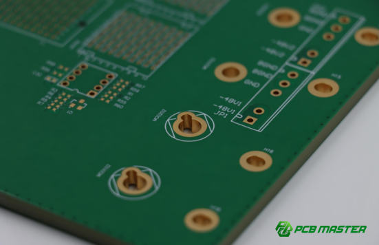
l Via opening size labeling: Designers should clearly mark the target copper openings in the PCB files. Properly dimensioned openings ensure that the laser can access the dielectric cleanly and that the microvia will be fully plated during electroplating.
Example: For a 100 μm microvia, marking a 300 μm target pad ensures full capture and avoids missed connections, even if slight misalignment occurs during drilling.
How should microvia design be optimized to improve manufacturing yield?
Optimizing microvia design involves selecting proper hole diameter, aspect ratio, pad size, via arrangement, and spacing. These factors ensure reliable plating, reduce defects, and maximize PCB manufacturing yield.
Laser hole diameter and aspect ratio (AR) design recommendations
Hole diameter and aspect ratio determine how easily a microvia can be drilled and plated.
l Recommended hole diameter and AR limits: Typical laser-drilled microvias range from 50–150 μm, with 75–100 μm being most common. The aspect ratio (hole depth to diameter) should ideally be ≤0.8:1 and never exceed 1:1 to prevent plating defects.
l Impact on plating: High aspect ratios make it difficult for copper to fully fill the via, leading to voids or incomplete connections. Lower aspect ratios allow better plating coverage and higher reliability.
Example: A 100 μm microvia in a 80 μm thick prepreg layer with a 0.8:1 AR ensures smooth plating and prevents empty spaces, while a 1.2:1 AR might trap air bubbles inside the via.
Pad size and alignment allowance planning
Pad size must account for via size and alignment tolerance to ensure proper electrical connection.
l Capture Pad vs. Finished Hole: The capture pad is the designed pad on inner layers, while the finished hole is the actual drilled hole after plating. The pad diameter should be at least 8–10 mils (200–250 μm) larger than the finished hole.
l Alignment tolerance: Sufficient pad size compensates for slight misalignments during drilling, preventing incomplete capture and potential open circuits.
Example: For a 100 μm finished hole, designing a 300 μm capture pad ensures that even if the laser is slightly off-center, the via still connects reliably.
Stacked vs. staggered via DFM strategies
The arrangement of microvias affects cost, yield, and reliability.
l Stacked via risks and costs: Stacked microvias align directly over each other. They require extremely precise layer registration and increase manufacturing complexity and cost. Misalignment can cause voids or connectivity issues.
l Staggered via advantages: Staggered microvias are offset across layers, reducing alignment challenges. This approach improves yield and reliability, making it the preferred choice for high-density boards.
Example: A 12-layer HDI smartphone PCB uses staggered microvias to connect multiple layers with minimal risk, whereas a stacked via design would increase cost by 20–30% and risk void formation.
Via edge and copper spacing requirements
Maintaining adequate distance between microvias and surrounding copper features prevents defects like short circuits and copper splatter.
l Minimum spacing recommendation: Keep at least 150 μm (6 mils) clearance from any adjacent copper traces, pads, or planes.
l Preventing copper splatter and shorts: Insufficient spacing can lead to copper debris during laser drilling, which may cause electrical shorts or reduce yield.
Example: On a dense HDI board, spacing microvias 150 μm away from nearby traces ensures clean laser drilling and reliable plated connections without additional rework.
How should PCB design files be prepared to ensure smooth laser drilling?
Accurate PCB design files are critical for laser drilling because they guide the drilling machine, define microvia locations, and prevent manufacturing errors. Proper stack-up, Gerber files, and drill file management ensure high yield and reliable microvias.
Accurate stack-up annotation
Clearly defining the PCB stack-up ensures the laser drills to the correct depth and connects the intended layers.
l Layer thickness and start/end layers: Each dielectric layer’s thickness must be precisely documented. Designers should also specify which layers the laser via starts and ends at, e.g., from L1 to L2 or L2 to L3. This information allows the laser to focus correctly and avoid over- or under-drilling.
Example: On a 10-layer HDI board, if the L3-L4 prepreg thickness is 80 μm, marking this in the stack-up ensures the laser drills the microvia exactly through the dielectric without damaging the adjacent copper layers.
Gerber file standards
Gerber files must clearly indicate where microvias are required and the associated pad structures to guide laser drilling and plating.
l Laser via areas and target pads: All microvia locations and their corresponding capture pads should be clearly defined in the Gerber layers. This prevents missing or misplaced vias during manufacturing.
l File naming and layer clarity: Use descriptive, unambiguous file names and ensure that layer order reflects the physical stack-up. Clear layer organization reduces confusion and errors at the fabrication stage.
Example: Naming the top layer Gerber as “L1_TOP_SIGNAL_GERBER” and laser via pad layer as “L1_L2_MICROVIA_GERBER” helps the manufacturer correctly interpret microvia placement.
NC Drill file separation management
Laser-drilled and mechanically drilled holes should be separated into different NC Drill files to avoid confusion and ensure proper drilling parameters are applied.
l Distinguishing laser vs. mechanical drilling: Laser microvias often have extremely small diameters (e.g., 0.1 mm) compared to mechanical vias. Separating these ensures correct machine settings and prevents damage to the board.
l Small drill number labeling: Use specific drill numbers or codes to clearly identify microvias, allowing the fabrication team to apply the correct laser settings for each type of via.
Example: An NC Drill file named “LASER_0.1MM_VIA.NC” for laser vias and “MECH_0.3MM_THROUGH.NC” for mechanical holes ensures no confusion in the drilling process.
What are the key considerations during the manufacturing process?
Successful laser drilling depends not only on design but also on careful control of manufacturing processes. Critical factors include dielectric thickness uniformity, layer alignment, desmearing, and copper plating quality. Each step affects microvia reliability and production yield.
Dielectric layer thickness and uniformity control
Uniform dielectric thickness is crucial for consistent laser drilling and complete microvias.
l Impact of thickness variation: If a dielectric layer is too thick or uneven, the laser may under-drill, leaving incomplete holes, or over-drill, damaging copper layers and creating irregular hole shapes. Maintaining consistent thickness ensures clean, fully formed microvias.
Example: In a 6-layer HDI board, a 5 μm variation in prepreg thickness can cause the laser to miss the target depth, resulting in incomplete vias. Strict material quality control prevents this issue.
Inner layer alignment accuracy and CTE compensation
Precise inner layer alignment is necessary to ensure microvias connect correctly between layers.
l Vision alignment systems: Laser drilling machines use cameras to detect inner layer pads for accurate positioning. High-resolution vision systems improve via placement precision.
l CTE (Coefficient of Thermal Expansion) compensation: During lamination, PCBs expand or shrink slightly. Compensating for this movement ensures the laser drills exactly where intended. Proper lamination and thermal control reduce misalignment risks.
Example: A smartphone PCB uses CTE-compensated lamination to ensure 100 μm microvias connect correctly across layers, even under thermal stress during pressing.
Desmearing and removal of resin residue
Removing residual resin and glass fibers from drilled holes is essential for proper copper adhesion.
l Potassium permanganate vs. plasma etching: Chemical desmearing with KMnO₄ oxidizes the residue, while plasma etching removes material using ionized gases. Both methods clean hole walls, but plasma is faster and avoids chemical waste.
l Hole wall roughness and hydrophilicity: Clean, slightly rough, and hydrophilic hole walls improve electroplating adhesion, ensuring fully filled and reliable microvias. Cross-section inspection verifies desmearing quality.
Example: Using plasma etching on VLP 1067 prepreg ensures smooth, clean microvia walls for high-yield plating. Over-etching, however, can enlarge the hole and reduce reliability.
Copper plating and via surface flatness
Proper copper plating fills microvias completely and maintains a flat surface for subsequent layer processing.
l Avoiding voids: Optimize plating solution, current density, and agitation to prevent trapped air pockets or voids inside microvias, which can cause electrical failure.
l Controlling dimplings: After plating, vias should be as flat as possible. Excessive dimpling can affect the next layer’s trace routing and reduce overall board reliability.
Example: On a high-density smartphone PCB, careful control of copper plating eliminates voids in 100 μm microvias and keeps via tops flush with the surface, ensuring smooth lamination of the next layer.
Conclusion
Mastering laser drilling for PCB microvias requires careful attention to material selection, microvia design, stack-up preparation, and precise manufacturing controls. Each decision—from dielectric choice and glass fabric type to pad sizing and alignment—directly impacts yield, reliability, and overall board performance. By understanding these critical factors, engineers can prevent defects such as voids, incomplete vias, and copper dimpling, ensuring high-quality HDI PCB production.
For companies seeking expertise in this complex process, PCBMASTER offers extensive experience in laser drilling DFM for microvias. Our team combines advanced equipment, precise process control, and deep design-for-manufacturing knowledge to deliver PCBs with optimal microvia quality, high reliability, and consistent yield. Whether you are designing high-density consumer electronics, automotive boards, or compact industrial PCBs, PCBMASTER ensures that your microvia drilling meets stringent performance standards while supporting efficient, scalable production.
With the right DFM strategies and a trusted manufacturing partner, your microvia designs can achieve both technical excellence and manufacturing efficiency, setting the foundation for next-generation PCB innovations.
FAQs
1. Is it feasible to have microvias smaller than 75 μm?
Microvias below 75 μm are technically possible but challenging. Smaller holes increase the risk of incomplete drilling and poor copper plating, especially in thicker dielectric layers. Maintaining precise laser focus and process control is critical, and production yield may decrease. Most HDI designs recommend 75–100 μm as a practical range.
2. Which is more reliable: stacked vias or staggered vias?
Staggered vias are generally more reliable. Stacked vias require extremely precise layer alignment and have a higher risk of voids or misregistration, increasing cost and manufacturing difficulty. Staggered vias offset across layers, improving yield and reducing the chance of plating defects.
3. How can residue on laser-drilled via walls be completely removed?
Residue can be removed using chemical desmearing with potassium permanganate (KMnO₄) or plasma etching. Plasma etching is faster and environmentally friendly, while KMnO₄ is a traditional method. Complete removal is verified by inspecting hole wall roughness and hydrophilicity to ensure good copper adhesion.
4. How does excessively thick copper foil affect laser drilling?
Thick copper increases the laser energy needed to open the via, which can cause overburning, irregular hole shapes, or reduced precision. Using ultra-thin copper (e.g., 1/3 oz or 12 μm) for outer layers reduces drilling difficulty and improves hole quality.
5. How can plated vias be checked for voids or dimpling?
Inspection is typically done using cross-section analysis or X-ray imaging. Cross-sectioning allows visual verification of voids and surface dimpling, while X-ray inspection detects internal voids without damaging the board. Proper monitoring ensures reliable, fully filled microvias.

