


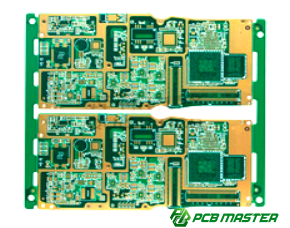
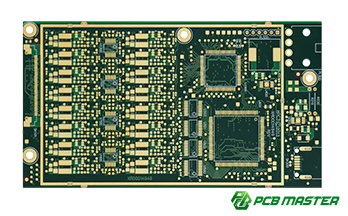
How to Ensure Precise Laser Blind Via Alignment in HDI PCB Manufacturing
Accurate alignment of laser blind vias is essential because even tiny misalignments can cause major electrical problems. If the vias do not line up perfectly between layers, the electrical resistance can increase, signals may degrade, or connections may fail entirely, leading to product scrap. In high-density interconnect (HDI) PCBs, where layers are tightly packed and spacing is extremely small, achieving micrometer-level alignment is not optional—it is mandatory for reliable performance.
High-precision alignment ensures that each laser-drilled via connects exactly to its target pad without overshoot or misplacement. For example, in a smartphone PCB with multiple stacked layers, a misaligned via could break the connection between the processor and memory, causing the device to malfunction.
As an experienced supplier of PCBs and PCBAs, PCBMASTER leverages advanced laser drilling technology, including real-time vision alignment and feedback control, to achieve sub-5-micron accuracy. By combining precise equipment, stable materials, and controlled processes, PCBMASTER minimizes errors, ensures reliable layer-to-layer connections, and maintains consistent production quality. This expertise is what enables high-end HDI PCBs to function flawlessly in demanding applications like 5G, wearable devices, and medical electronics.
How Can High-Precision Equipment and Core Technologies Improve Blind Via Alignment?
High-precision equipment and core technologies are crucial for achieving micro-level alignment in blind vias. They ensure that each via connects perfectly between layers, reducing defects and improving PCB reliability.
What Role Does a High-Precision Laser Drilling Machine Play?
A high-precision laser drilling machine ensures that blind vias are drilled accurately and consistently.
CCD Visual Alignment System: Modern laser drills use CCD cameras to scan alignment targets on the PCB. This system measures the exact position of the board and calculates any movement or distortion. With this, machines can position each via with a ±5μm precision. For example, even if a PCB slightly stretches during lamination, the CCD system detects it and adjusts the drilling path.
Real-Time Focus Control: The laser’s focus must remain stable throughout drilling. If the focus drifts, the via shape can distort, causing poor electrical connections. Real-time focus control continuously adjusts the laser, ensuring every via is clean and uniform, which is critical for high-density interconnects (HDI) PCBs.
Why Is LDI (Laser Direct Imaging) Technology Important?
LDI replaces traditional photo masks to create highly accurate PCB patterns.
Eliminates Mask Alignment Errors: Traditional photolithography uses physical masks, which can warp or shift. This introduces small but critical errors in layer alignment. LDI directly exposes the photoresist with a laser guided by digital design files, removing mask-based misalignment.
Ensures Precise L2 Pad and Trace Placement: By accurately forming the L2 layer pads and traces, LDI sets a precise reference for subsequent blind via drilling. For example, when drilling a via from L1 to L2, the exact pad position ensures the via lands perfectly, reducing the risk of electrical failure.
How Does Automated Optical Inspection (AOI) Ensure Process Control?
AOI detects and corrects deviations during key PCB manufacturing steps.
Via Position Scanning: After processes like inner layer etching or first-level via plating, AOI scans every via for position and size accuracy. It creates a digital map of any deviations.
Immediate Feedback and Adjustment: If AOI detects misaligned vias, the system alerts operators or adjusts the next laser drilling step. For instance, in a multi-layer HDI PCB, AOI ensures that the first drilled vias provide a reliable reference for the second drilling, maintaining micro-level alignment across layers.
How Can Precise Process Design and Control Achieve Micron-Level Alignment?
Micron-level alignment in blind vias is achieved by combining optimized alignment targets, carefully controlled plating, strategic drilling sequences, and precise laser settings. Each step ensures that the next layer aligns perfectly.
How Does Optimized Alignment Target Design Improve Via Accuracy?
Alignment targets guide the laser drilling machine to position vias correctly, compensating for board movement.
Global and Local Target Combination: Global targets at the board edges measure overall shift, rotation, or stretching. Local targets inside the board measure small distortions in specific areas. Using both ensures accurate via placement across the entire PCB.
Software Compensation for Board Changes: The system calculates the PCB’s expansion, shrinkage, or rotation and automatically adjusts drilling coordinates. For example, if a 100 mm board stretches by 0.02 mm, the software shifts drilling positions to maintain perfect alignment. This ensures that blind vias land precisely, even after lamination or heat exposure.
Why Is First-Level Via Plating and Filling Critical?
Filling first-level vias with copper creates a stable, flat surface for the second drilling step.
Provides a Flat Starting Point: Unfilled vias leave small depressions that scatter the laser, causing misalignment. Fully filled vias prevent scattering and allow the laser to hit the target accurately.
Ensures Precise Second-Level Drilling: Using filled vias as reference points helps the second laser drilling step land perfectly on the next layer. For example, L1 vias filled with copper provide the base for L2 drilling, maintaining micron-level alignment throughout the HDI PCB.
What Is the Strategy Between Two Drilling Steps?
Controlling the sequence and alignment of multiple drilling steps ensures accurate layer-to-layer connections.
L1→L2 Drilling: The first drilling uses L2 layer alignment targets as a reference, ensuring that vias connect the first and second layers correctly.
L2→L3 Drilling:
l Board Flipping and High-Precision Scanning: After lamination, the board is flipped, and targets are scanned again to measure any movement or distortion.
l Using First-Level Vias as Ultimate Reference: The actual position of the filled first-level via guides the second laser drilling. This dynamic correction accounts for any thermal or mechanical shifts, ensuring the second via connects perfectly.
How Can Laser Parameters Be Optimized for Accuracy?
Adjusting laser energy and pulse frequency according to material type ensures clean, precise vias.
Material-Based Adjustment: Copper, prepreg (PP), and dielectric layers respond differently to laser energy. Using the correct settings prevents over-drilling or under-drilling.
Ensures Drilling Stops at Target Layer: Proper settings allow the laser to stop exactly on the target copper layer, providing clean edges and maintaining alignment. For example, too much energy can burn the dielectric, while too little leaves residue, both of which can cause misalignment in HDI PCB vias.
How Can Stable Material Systems Reduce Alignment Errors?
Using stable materials and precise lamination techniques minimizes PCB warping or shrinking, ensuring blind vias and layers stay accurately aligned.
Why Are Low-Shrinkage Core Boards Important for Alignment?
Low-shrinkage core boards maintain their size during heating and lamination, reducing layer misalignment.
Core boards can expand or contract slightly when exposed to heat or pressure. Even a tiny movement of a few microns can misalign blind vias. Using materials with low thermal expansion, like FR-4 variants with controlled coefficient of thermal expansion (CTE), ensures that the PCB keeps its original dimensions. For example, a 0.5% shrinkage on a 100 mm board could cause a 0.5 mm misalignment—enough to break micro-via connections. By using low-shrinkage cores, PCBMASTER ensures the vias stay in precise positions throughout the manufacturing process.
How Does a Symmetrical Lamination Structure Reduce Cooling Stress?
Symmetrical layer arrangements balance internal stresses, preventing warping during cooling.
If a PCB stack-up is asymmetrical, one side may cool faster or shrink more, causing bending or twisting. Symmetrical lamination, with identical material thicknesses and copper distribution on both sides, balances stress evenly. This keeps the board flat, maintaining accurate via alignment. For instance, an HDI PCB with uneven copper layers could warp during cooling, shifting vias by tens of microns. Symmetrical design avoids this problem, supporting micron-level precision.
Why Is Precise Control of Lamination Temperature, Pressure, and Time Critical?
Consistent lamination conditions prevent uneven resin flow or board distortion, which could misalign layers.
During lamination, prepreg layers soften and bond under heat and pressure. If the temperature rises too fast, or pressure is uneven, the resin can flow irregularly, causing local board expansion or contraction. By controlling temperature ramp-up, holding pressure, and lamination time precisely, manufacturers ensure uniform layer bonding and minimal distortion. For example, a controlled lamination cycle keeps HDI PCBs flat and stable, making the blind via positions reliable across the board.
How Can Strict Production Management Maintain Via Accuracy?
Strict production management ensures stable conditions, controlled workflows, and continuous quality monitoring, all of which prevent misalignment in blind vias and maintain micron-level precision.
Why Is Environmental Control Important for Via Alignment?
Maintaining constant temperature and humidity prevents material deformation that can misalign vias.
PCB materials expand or contract when exposed to temperature or humidity changes. Even small variations can cause layer shifts of several microns, affecting blind via connections. By keeping the production workshop at a stable temperature and humidity—commonly ±1°C and ±5% RH—PCBMASTER ensures that boards stay flat and consistent. For example, a board stored in a humid environment may swell slightly, causing laser drilling to miss its target. Controlled environmental conditions eliminate this risk, supporting precise layer-to-layer alignment.
How Does Workflow Control Ensure Consistent Via Accuracy?
Standardized process steps and controlled dwell times reduce deviations caused by human error or material stress.
Each stage of PCB manufacturing—lamination, drilling, plating—must follow strict timing and operational rules. Delays or improper handling can allow boards to bend, expand, or cool unevenly. PCBMASTER enforces workflow protocols, including defined handling, storage, and processing times for each batch. For instance, limiting the time a board spends between lamination and drilling prevents heat-induced expansion, keeping vias aligned. This careful workflow control ensures repeatable, micron-level precision across large production runs.
Why Are First-Article Inspection and SPC Critical for Alignment?
First-article inspection and Statistical Process Control (SPC) detect deviations early and prevent defective batches from progressing.
First-article inspection involves cutting sample boards and examining them under a microscope to verify via positions, shapes, and connectivity. SPC continuously tracks key metrics such as via diameter, offset, and layer alignment, generating alerts if trends show potential misalignment. For example, if SPC detects gradual shifting of vias in a batch, the process can be adjusted before more boards are drilled. This feedback loop ensures consistent quality, prevents defects, and maintains high alignment accuracy in HDI PCBs.
What Is PCBMASTER’s High-Precision Blind Via Alignment Logic Chain?
PCBMASTER achieves micro-level blind via alignment through a step-by-step process that combines stable materials, precise imaging, high-precision drilling, real-time correction, and feedback verification.
How Does Material Stability and LDI Imaging Form Precise Targets?
Stable PCB materials combined with Laser Direct Imaging (LDI) create accurate alignment targets that guide subsequent drilling steps.
Materials with low thermal expansion and minimal shrinkage ensure that the PCB maintains its size during processing. LDI directly exposes the copper and photoresist layers using digital files, eliminating errors from traditional masks. Together, these create precise global and local targets that define exactly where blind vias should be drilled. For example, on an HDI PCB, these targets allow the first via to align within ±5μm, providing a reliable foundation for later layers.
How Do High-Precision Laser Machines and AOI Complete First-Level Via Fabrication?
Laser drilling machines with CCD alignment systems and real-time focus, combined with Automated Optical Inspection (AOI), ensure the first-level vias are drilled accurately.
After the targets are set, the laser drills the first via with micron-level precision. AOI then scans the vias to check size, position, and quality. Any deviations are immediately flagged, ensuring that only perfect first-level vias serve as the reference for the second-level drilling. This step guarantees consistent alignment across multiple layers in complex HDI PCBs.
How Is the First-Level Via Position Used to Correct Second-Level Drilling?
The actual position of first-level vias acts as a dynamic reference to adjust the second-level drilling coordinates.
After the board undergoes lamination and thermal processes, minor shifts may occur. PCBMASTER measures the exact location of filled first-level vias and uses this data to compensate the second laser drilling. This ensures that the second via connects perfectly with the first, achieving micron-level alignment. For example, even if the board shifts by 10 μm, the system recalculates the drilling path, preventing misalignment and maintaining high yield.
How Does Cross-Section Verification Create a Closed Feedback Loop?
Cross-section inspection validates via alignment and feeds results back to optimize the process.
Sample boards are cut and observed under a microscope to confirm that vias meet the alignment specification. If small deviations are detected, the process parameters—such as laser focus, target calibration, or material handling—are adjusted for the next batch. This closed-loop feedback ensures continuous improvement, guaranteeing consistent high-precision blind via placement in all PCBMASTER HDI production runs.
Conclusion
In high-density HDI PCB manufacturing, precise blind via alignment is not a single-step task—it is a system-wide commitment. From using stable, low-shrinkage materials and advanced LDI imaging to employing high-precision laser drilling, AOI inspection, and carefully optimized process controls, every step ensures micron-level accuracy. By leveraging first-level via positions as dynamic references and validating results through cross-section feedback, PCBMASTER consistently achieves flawless layer-to-layer connectivity.
This meticulous approach minimizes electrical failures, reduces scrap rates, and guarantees reliable performance for complex electronic applications. For engineers and designers, understanding this logic chain highlights the value of integrating material science, cutting-edge equipment, and strict production management in modern PCB fabrication.
At PCBMASTER, we combine expertise, technology, and rigorous process control to deliver high-quality HDI PCBs that meet the most demanding precision standards. Whether you’re developing advanced consumer electronics, aerospace systems, or medical devices, our approach ensures that your designs connect perfectly, every time.
Precision is not an option—it is the foundation of performance, and PCBMASTER is committed to making it a reality.
FAQs
1. Why Does Traditional Optical Imaging Often Cause Blind Via Misalignment?
Traditional optical imaging relies on physical masks to transfer PCB patterns. Masks can warp, stretch, or shift slightly during processing, introducing small but critical alignment errors. These tiny deviations accumulate across layers, causing blind vias to miss their target pads. In contrast, laser direct imaging (LDI) eliminates mask-related errors, providing precise layer alignment for HDI PCBs.
2. How Can You Determine If Second-Level Blind Vias Achieve Micron-Level Alignment?
Micron-level alignment can be verified using automated optical inspection (AOI) and cross-section analysis. AOI scans measure via positions relative to reference pads, while cross-section inspection under a microscope confirms exact layer-to-layer connectivity. If via offsets are within ±5 microns, the alignment meets high-precision HDI standards.
3. Why Is Filling First-Level Vias Important in High-Density HDI PCBs?
Filling first-level vias with copper creates a flat, stable surface for second-level drilling. Unfilled or partially filled vias leave depressions that scatter the laser, reducing accuracy. Filled vias provide a reliable reference, ensuring the second drilling step lands precisely, which is critical for micron-level layer-to-layer connections.
4. How Much Does Material Shrinkage Affect Laser Drilling Accuracy?
Even tiny material expansion or contraction can misalign blind vias by several microns. For example, a 0.5% shrinkage on a 100 mm PCB could shift via positions by 0.5 mm, enough to break connectivity. Using low-shrinkage core materials minimizes distortion, maintaining laser drilling precision and ensuring accurate via placement.
5. How Does PCBMASTER Use Process Control to Reduce Production Deviations?
PCBMASTER maintains strict workflow protocols, environmental controls, and statistical process monitoring (SPC). Consistent temperature, humidity, handling procedures, and dwell times prevent board deformation. First-article inspections and SPC detect deviations early, allowing real-time adjustments. This ensures stable, repeatable blind via alignment across every production batch.

