


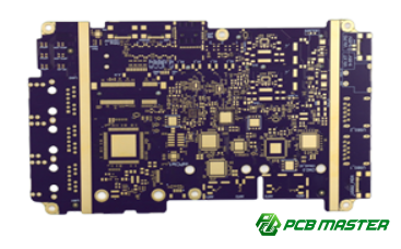
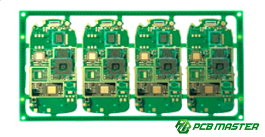
Common HDI PCB Manufacturing Problems and How to Fix Them
High-Density Interconnect (HDI) PCBs are essential for modern electronics, enabling smaller, faster, and more reliable devices. Manufacturing them, however, is highly demanding—tiny variations in materials, equipment, or processes can lead to defects that affect performance and durability.
Understanding the common challenges at each stage of HDI production is key to preventing issues and ensuring consistent quality. From inner-layer circuitry to laser-drilled microvias, from copper-filled holes to surface finishes, each step requires careful control and optimization.
This guide from PCBMASTER highlights frequent HDI manufacturing problems and provides practical strategies to address them. By following these insights, engineers and manufacturers can improve yields, reduce rework, and produce boards that meet strict performance and reliability standards.
What Are Common Inner-Layer Core Problems in HDI PCB Manufacturing and Their Solutions?
Inner-layer cores are the foundation of HDI PCBs. Defects at this stage can cause serious issues in later production steps, affecting electrical performance and reliability. Common problems include open circuits, short circuits, and poor line quality. Understanding why these problems happen and how to prevent them is essential for successful HDI manufacturing.
What Causes Inner-Layer Circuit Defects (Open and Short Circuits)?
Open circuits and short circuits in inner layers usually happen due to misaligned images, uneven exposure, incorrect chemical settings, or dirty copper surfaces.
l Photomask Distortion: If the photomask or film used to transfer the circuit pattern is bent or stretched, the resulting lines may break or merge incorrectly. This can lead to open circuits (broken paths) or short circuits (unintended connections). Real-world example: In a small smartphone PCB, a bent film caused several micro-traces to short, triggering functional failures.
l Incorrect Exposure Energy: If the UV light during exposure is too strong or too weak, the photoresist does not fully harden in the right areas. This leads to missing lines (open circuits) or residual unwanted copper (short circuits).
l Poor Development or Etching Parameters: Using incorrect chemical concentrations, temperatures, or timing during development or etching can damage line integrity. Lines may erode or remain connected where they shouldn’t.
l Dirty Copper Surface: Oxidation, dust, or residue on copper can prevent the photoresist from adhering properly, causing incomplete patterns and defects in the inner layer.
How to Fix Inner-Layer Circuit Defects
Control environment, calibrate equipment, optimize chemicals, and keep copper surfaces clean to reduce open and short circuits.
l Strict Temperature and Humidity Control: Maintain a stable environment during exposure and processing. High humidity or temperature swings can distort the photomask and the core board, causing misalignment. Using high-precision photomasks or LDI (Laser Direct Imaging) can reduce errors caused by film distortion.
l Regular Exposure Calibration: Measure and adjust UV exposure energy frequently. This ensures the photoresist hardens exactly as intended, preventing missing lines or extra copper deposits.
l Optimized Etching Parameters: Adjust etching speed, pressure, and chemical concentrations to match board specifications. Conduct initial tests (first-piece inspections) to verify line accuracy before full production.
l Enhanced Surface Preparation: Clean copper thoroughly using chemical cleaning or plasma treatment to remove oxidation and debris. This ensures good adhesion of photoresist and accurate line formation.
Example: A PCB manufacturer reduced inner-layer shorts by 80% after switching to LDI and strict copper cleaning procedures, showing how small process improvements lead to major quality gains.
How to Solve Common Problems in the Laser Drilling Process?
Laser drilling is a critical step in HDI PCB manufacturing. Microvias created by lasers connect different layers of the PCB. If these microvias are not precise or clean, they can cause electrical failures or reduce reliability. Common issues include poor hole shape, copper or resin residues, and misregistration (misalignment).
Why Do Poor Hole Shapes Occur and How Can They Be Optimized?
Poor hole shapes, like uneven or non-circular microvias, occur when laser settings or support materials are not correct. Optimizing parameters and using proper support can improve hole quality.
l Incorrect Laser Settings: Laser energy, frequency, or pulse count that is too high or too low can create holes that are too wide, narrow, or tapered unevenly. Example: A smartphone PCB had microvias with tapered sides due to excessive pulse count, causing poor plating in the next step.
l Inappropriate Support Material: The backing layer (called a “pad” or “dummy board”) must absorb excess laser energy. If the material or thickness is wrong, the board can burn, deform, or produce irregular holes.
l DOE (Design of Experiments) Optimization: Running small-scale tests to systematically adjust laser parameters helps find the balance between drilling speed and hole quality.
Proper Pad Material Selection: Choosing a compatible pad material ensures stable drilling, reduces burrs, and maintains microvia shape.
How to Reduce Copper Smear and Resin Residue
Copper and resin residues occur when laser energy melts materials unevenly. Proper laser control and post-drilling cleaning are needed.
l Laser Parameter Optimization: Adjust energy, frequency, and pulse to minimize overheating. For boards with copper on the surface, a two-step drilling method—burn copper first, then burn resin—can prevent residues.
l Flat Drill Pad Support: Ensure the pad under the PCB is flat and stable. This prevents vibrations that can smear copper or create resin droplets on the hole walls.
l Enhanced Post-Drill Cleaning (Desmear): Use chemical cleaning or plasma treatment to remove any remaining copper or resin from microvias. This ensures reliable plating and prevents open or short circuits later.
Example: A manufacturer reduced resin residue by 70% after switching to two-step drilling with improved pad support.
How to Correct Misregistration (Hole Misalignment)
Misregistration happens when drilled holes don’t match inner-layer targets. Measuring material expansion and using precise equipment prevents this.
l Measure Core Expansion: HDI cores expand or shrink during processing. Measuring this and adjusting drilling programs ensures holes are aligned correctly.
l High-Precision CCD Cameras and Calibration: Using cameras to detect alignment markers and regularly calibrating the laser drill ensures accurate targeting.
l Control Temperature and Humidity: Stable environmental conditions prevent board deformation, keeping microvias in the correct positions.
Example: Controlling humidity in a PCB factory reduced misregistration defects by 50%, improving yield in high-density boards.
What Are Common HDI Via Metallization Problems and How to Optimize Filling?
Via metallization, or copper filling, is a critical step in HDI PCB manufacturing. Microvias must be completely filled with copper to ensure electrical reliability. Common problems include incomplete filling (voids) and defects at the via openings such as recesses or dog-boning. Proper control of plating chemistry, current, and cleaning is essential for high-quality vias.
Why Do Voids Occur in Microvias and How Can They Be Improved?
Voids in microvias happen when copper does not fully fill the hole, usually due to chemical, electrical, or surface issues. Optimizing plating solution, current, and cleaning prevents these gaps.
l Inactive Plating Solution: If the copper plating solution or its additives are weak or degraded, copper does not deposit evenly, leading to empty spaces in the via. Using specialized via-fill chemicals and monitoring additive activity ensures consistent copper deposition.
l Incorrect Current Density or Waveform: Applying too much or too little current, or using the wrong waveform, can cause copper to build unevenly. Step-current plating—starting with low current for the via walls and increasing for filling—promotes uniform deposition.
l Dirty Via Walls: Contaminants on the via surface trap air bubbles, preventing copper from filling the hole completely. Proper pre-treatment, cleaning, and activation of the via wall improve adhesion and void-free filling.
l Ultrasonic or Vibration Assistance: Using gentle vibration or ultrasonic agitation during plating helps air bubbles escape, ensuring complete copper filling.
Example: A manufacturer reduced microvia voids by 60% after switching to step-current plating with ultrasonic agitation and carefully monitored additive levels.
How to Prevent Via Recesses and Dog-Boning
Recesses or dog-boning occur when copper overfills inside the via but does not form a level surface, often due to uneven plating. Adjusting current and post-processing fixes this.
l Optimize Plating Current and Additives: Using leveling additives in the plating solution and adjusting current waveforms helps copper deposit more evenly. This prevents excessive buildup at the via edges.
l Post-Fill Planarization: After filling, techniques like chemical-mechanical polishing (CMP) or selective etching remove excess copper from the via opening. This creates a flat surface, ready for accurate outer-layer patterning.
Example: In high-density smartphone PCBs, applying planarization after optimized plating eliminated dog-boning defects, improving solder joint reliability on subsequent assembly.
How to Handle Common Outer-Layer Patterning and Etching Problems?
Outer-layer patterning and etching are crucial for final HDI PCB functionality. Poor alignment or rough lines can cause short circuits, open circuits, or unreliable soldering. Common problems include misalignment of the outer layer and line defects like rough edges or missing traces. Controlling board expansion, exposure precision, and surface flatness helps achieve high-quality outer-layer circuits.
Why Does Outer-Layer Misalignment Occur and How Can It Be Corrected?
Misalignment happens when the outer-layer pattern does not match inner layers, often due to board expansion or equipment inaccuracies. Measuring board changes and using precise imaging equipment corrects this.
l Board Expansion After Lamination: HDI boards expand or shrink slightly after lamination due to heat and pressure. Without compensation, outer-layer patterns may shift. Measuring these changes and adjusting the pattern in the CAD/CAM software before exposure can prevent misalignment.
l Exposure Equipment Limitations: LDI (Laser Direct Imaging) machines or traditional exposure systems may have slight positioning errors. Regular calibration and using high-precision LDI machines minimize alignment errors.
l Compensation Through Measurement: Track dimensional changes after lamination and feed the data back into pattern generation to correct offsets. This ensures outer-layer traces line up perfectly with inner layers.
l Use of LDI Technology: Switching from film-based photomasks to LDI eliminates errors from film deformation, providing more accurate alignment for high-density boards.
Example: A PCB manufacturer using LDI reduced outer-layer misregistration defects by 60% compared to traditional film exposure.
How to Reduce Line Gaps and Rough Edges (Rough Lines)
Rough lines and gaps occur when the surface is uneven or etching is not controlled. Flattening the board and using precise materials and chemicals produces smooth traces.
l Flatten the Surface After Via Filling: After microvia filling, the board surface may be uneven. Processes like chemical-mechanical polishing (CMP) or surface etching help create a flat surface, which ensures uniform exposure and accurate trace formation.
l Use High-Resolution Dry or Wet Films: High-resolution photoresists improve pattern fidelity. Dry films or advanced wet films allow finer line widths with fewer defects, especially on dense HDI boards.
l Optimize Etching Parameters: Adjust chemical concentration, temperature, etching time, and agitation to reduce side-etching. Proper control prevents rough edges and ensures trace widths match design specifications.
Example: By combining surface flattening with high-resolution dry film and controlled etching, a manufacturer eliminated over 70% of rough-line defects in a 0.15 mm line HDI board.
How to Prevent Common Defects During HDI PCB Lamination?
Lamination is the process of bonding multiple layers of the HDI PCB together under heat and pressure. Poor lamination can cause delamination (layers separating) or whitening defects, which reduce electrical reliability and mechanical strength. Preventing these defects requires attention to material quality, cleanliness, and process control.
What Causes Delamination and Whitening Between Layers?
Delamination and whitening happen when layers do not bond properly. This is usually due to contamination, improper lamination settings, or incompatible or expired materials.
l Insufficient Cleanliness Before Lamination: Dust, oils, or residues on core boards or prepreg sheets prevent proper bonding. Even tiny particles can trap air, causing white spots or separation between layers.
l Incorrect Lamination Parameters: Temperature, pressure, vacuum level, or duration that are too high or too low can lead to incomplete resin flow or curing. Poor resin distribution can leave gaps or weakly bonded areas.
l Material Mismatch or Expired PP/Prepreg: If the resin content of prepreg (PP) or core boards is too high, too low, or expired, the layers will not bond properly. The wrong combination can also lead to uneven curing, causing whitening or delamination.
Example: A manufacturer experienced repeated delamination on 8-layer HDI boards due to expired prepreg sheets. Replacing them solved the issue immediately.
How to Improve Lamination and Avoid Defects
Control cleanliness, optimize lamination settings, and verify materials to prevent delamination and whitening.
l Strict Environmental Control: Maintain clean lamination rooms with controlled humidity and dust-free conditions. This reduces contamination that can interfere with resin bonding.
l Optimized Lamination Curve: Adjust temperature, pressure, vacuum, and time to allow resin to flow fully and cure completely. This ensures strong adhesion between layers and eliminates trapped air.
l Enhanced Incoming Material Inspection: Verify the quality, resin content, and expiration of PP sheets and core boards before use. Matching resin content with core board specifications ensures proper bonding and uniform curing.
Example: After implementing strict environmental control and material inspection, a PCB factory reduced lamination defects from 8% to less than 1%, improving yield for multi-layer HDI boards.
How to Prevent Surface Finish Problems in HDI PCB Manufacturing?
Surface finish is the final step that protects copper traces and ensures reliable soldering. One of the most common issues with ENIG (Electroless Nickel Immersion Gold) finishes is Black Pad, which can lead to poor solder joints or connection failures. Preventing this defect requires precise control of chemical baths and process timing.
What Causes ENIG Black Pad Formation?
Black Pad occurs when the nickel layer is improperly plated or over-oxidized during the gold plating process.
l Abnormal Phosphorus Content in Nickel Layer: ENIG uses electroless nickel with a small percentage of phosphorus to improve corrosion resistance. If the phosphorus level is too high or too low, the nickel layer may be brittle or uneven, making it susceptible to black pad during gold immersion.
l Over-Corrosion or Oxidation During Gold Plating: If the nickel layer is attacked too aggressively during immersion gold plating, or if it oxidizes while waiting between processes, a darkened, non-solderable surface forms. This is the classic Black Pad defect, causing weak solder joints and poor reliability.
Example: A manufacturer found solder failures on HDI boards traced to high phosphorus levels in nickel. Correcting the phosphorus concentration resolved the Black Pad issue.
How to Improve ENIG Process and Prevent Black Pad
Control chemical properties, optimize gold plating, and minimize nickel exposure to air between steps.
l Strict Control of Nickel Bath: Monitor and maintain nickel bath temperature, pH, and phosphorus content. Consistent chemical composition ensures uniform, durable nickel deposition, reducing the risk of Black Pad.
l Optimize Gold Immersion Process: Adjust immersion time and bath composition to deposit gold evenly without over-corroding the nickel. This produces a smooth, solderable surface.
l Reduce Waiting Time Between Steps: Minimize the time the nickel layer is exposed to air or storage. Less exposure reduces oxidation risk, which is a key factor in Black Pad formation.
Example: By maintaining nickel pH and temperature and streamlining plating steps, a PCB factory reduced Black Pad defects by over 80%, ensuring stronger solder joints on high-density boards.
How to Systematically Improve Overall HDI PCB Manufacturing Quality?
Achieving high-quality HDI PCBs requires a systematic approach that goes beyond fixing individual defects. Quality must be built into the design, monitored during production, supported by reliable equipment and materials, and reinforced through a culture of awareness among all personnel.
How Can Design Optimization (DFM) Improve HDI Manufacturing?
Optimizing PCB design for manufacturability (DFM) reduces defects from the source by considering material behavior and process limitations.
l Avoid Drilling Holes at Pad Edges: Placing vias too close to solder pads can weaken connections or cause short circuits. Ensuring proper spacing minimizes stress during lamination and drilling.
l Maintain Proper Trace Width and Spacing: Balanced line widths and spacing prevent over-etching, short circuits, and reliability issues in high-density boards.
l Balance Copper Distribution to Reduce Warpage: Uneven copper can cause board bending during lamination or heat exposure. Proper copper layout minimizes mechanical stress and reduces lamination or drilling defects.
Example: A smartphone PCB redesign that moved vias away from pads and balanced copper layers reduced lamination warpage by 40% and lowered via defects.
How Does Strict Process Control and Monitoring Enhance Quality?
Monitoring key processes ensures stable production and reduces variability that causes defects.
l Establish SOPs and Monitor Key Parameters: Standard operating procedures ensure consistent execution for steps like laser drilling, plating, and etching. Tracking temperature, pressure, and chemical concentrations prevents process drift.
l Use Statistical Process Control (SPC): SPC analyzes production data in real-time to detect trends or deviations. Early alerts allow immediate adjustments, improving yield and consistency.
Example: Implementing SPC on laser drilling lines reduced microvia misregistration by 50% in a high-volume HDI production line.
How Can Equipment Maintenance and Material Management Prevent Defects?
Reliable equipment and proper material handling ensure processes perform as designed without unexpected failures.
l Regular Preventive Maintenance and Calibration: Laser drills, plating lines, LDI machines, and laminators must be maintained and calibrated to prevent errors from worn parts or misalignment.
l Material Management System: Track board cores, prepreg sheets, plating chemicals, and films to ensure they are within shelf life and stored under correct conditions. This avoids defects caused by expired or improperly stored materials.
Example: A PCB factory reduced ENIG Black Pad defects by 70% after implementing systematic chemical tracking and laser drill calibration.
How Does Promoting a Quality-Aware Workforce Improve HDI Manufacturing?
A culture of quality ensures problems are detected and corrected quickly, preventing larger failures.
l Implement Total Quality Management (TQM): Integrate quality checks into every stage, from material inspection to final testing.
l Encourage Operator Feedback: Operators closest to production can identify potential issues early. Timely reporting allows corrective actions before defects propagate.
Example: After TQM training and feedback systems were established, a PCB assembly line reduced defect rates by 30%, demonstrating the impact of staff engagement on quality.
Conclusion
Ensuring high-quality HDI PCB manufacturing requires more than fixing isolated problems—it demands a holistic approach that combines careful design, precise process control, reliable equipment, proper materials, and a culture of quality awareness. By understanding common defects and implementing systematic improvements, manufacturers can significantly reduce failures, improve yields, and deliver reliable, high-density boards for modern electronics.
For companies looking for expert guidance and reliable HDI PCB solutions, PCBMASTER offers comprehensive support, from design optimization to production excellence, helping clients achieve consistent quality and high-performance results.
FAQs
1. Why does resin residue often appear during HDI microvia drilling?
Resin residue occurs when laser drilling melts part of the dielectric material (resin) inside or around the microvia. If the laser energy or pulse settings are too high, or if the supporting drilling pad is uneven, melted resin can reattach to via walls or the bottom copper surface. Optimizing laser parameters, using a two-step drilling method (copper first, resin second), and applying post-drilling cleaning like desmear or plasma treatment can significantly reduce resin residue.
2. Why does Black Pad occur on ENIG surfaces?
Black Pad happens when the nickel layer is improperly plated or over-oxidized during immersion gold plating. Key causes include abnormal phosphorus content in the nickel, over-corrosion of nickel during gold deposition, or oxidation while waiting between process steps. Controlling nickel bath pH, temperature, phosphorus level, and minimizing exposure to air reduces the risk of Black Pad, ensuring reliable soldering and long-term connectivity.
3. Can via filling voids (Voids) be completely avoided?
Voids cannot always be fully eliminated, but they can be minimized. Causes include insufficient plating solution activity, improper current density, and poor via-wall cleanliness. Using specialized via-fill chemicals, step-current plating, proper pre-treatment, and ultrasonic or vibration-assisted plating improves copper filling and greatly reduces voids. Consistent monitoring and optimized process parameters help achieve near-void-free microvias in most production scenarios.
4. How can rough lines on outer-layer traces be minimized from the source?
Rough lines often result from uneven surfaces, improper exposure, or suboptimal etching. Flattening the board after microvia filling, using high-resolution dry or wet films, and controlling etching parameters (chemical concentration, temperature, time, and agitation) reduce side etching and produce smooth, uniform traces. Early attention during design and surface preparation helps prevent rough edges before exposure and etching even begins.
5. What is the difference between lamination whitening and delamination, and how can they be prevented?
Whitening is a visible discoloration caused by trapped air or moisture between layers, while delamination is the actual separation of layers, affecting mechanical and electrical integrity. Both arise from poor cleanliness, improper lamination temperature/pressure/vacuum/time, or incompatible or expired prepreg and core materials. Prevention involves strict cleanroom control, optimized lamination curves for full resin flow and curing, and careful incoming material inspection to ensure compatibility and quality.

