






EV DC/DC Converter PCB Design: A Complete Guide for Automotive Applications
Efficient power conversion is a prerequisite for the reliable operation of the critical low-voltage systems in electric vehicles. The key element of this process is the DC/DC converter. But stable performance involves more than simply choosing the right power components. A well designed PCB directly influences current capability, electrical isolation, thermal performance, electromagnetic compatibility and long term reliability in harsh automotive environments.Furthermore, as EV platforms demand higher voltage, higher power density and smaller form factors, PCB design becomes a critical element in the overall performance and manufacturability of the converter. Whether designing a new automotive power converter or optimizing an existing design, you need to understand the PCB-specific design considerations. This guide provides an overview of the basic principles, design techniques, and manufacturing challenges associated with the design of reliable EV DC/DC converter PCBs for automotive applications.
What Is an EV DC/DC Converter PCB and How Does It Work?
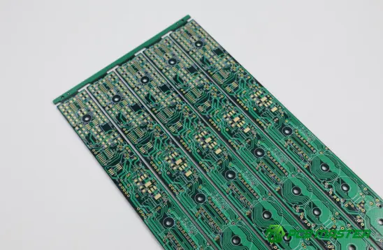
In an EV DC/DC converter , the PCB is the printed circuit board that holds and connects all the electronic components inside the DC/DC converter . It distributes power, controls switching circuits and signals and makes voltage conversion efficient, stable and reliable in electric cars.
The EV DC/DC converter PCBs need to work in more severe automotive environments, compared with traditional power supply PCBs, with higher voltage and higher current. It must also meet strict requirements for electrical isolation, thermal performance, electromagnetic compatibility (EMC) and long-term reliability. With the technology of EVs moving to higher power density and 800V architecture, PCB design is becoming an important factor of the performance of the converter, and not just a platform to mount the components.
The role of a DC/DC converter in electric vehicles
EV battery is a high voltage battery. Then, a DC/DC converter is used to step down the voltage to a lower voltage and is used to power the electrical systems on the vehicle.
The average electric car's main battery pack is 400V or 800V, while most of the vehicle's electronics are 12V or 48V. DC/DC converter to bring the voltages down to these lower levels. This allows to safely reduce the battery voltage to these lower levels without wasting much power .
The energy converted is used to run many vital functions on the vehicle such as:
- Headlights and interior lighting
- Infotainment systems
- Digital instrument clusters
- Power steering
- Electric water pumps
- Cooling fans
- Electronic control units (ECUs)
These low voltage systems cannot be directly supplied from the high voltage battery without a DC/DC converter.
For instance, while an EV is driving on the highway, the traction battery is powering the electric motor and the DC/DC converter is constantly providing steady 12V power to the vehicle's control modules and accessories. This allows the high and low voltage electrical systems to work together safely and efficiently.
How an EV DC/DC converter PCB enables power conversion
The PCB provides the electrical connections and current paths and control circuits that the DC/DC convertor needs to efficiently and reliably convert voltage.
A typical DC / DC converter consists of many electronic components including power MOSFET or SiC MOSFET, transformer or inductor, capacitor, controller and sensor. The components are interconnected on the PCB to form a complete power conversion circuit.
Most importantly, the PCB is not just a mounting board but part of the electrical design. The layout affects the current flow, switching performance, heat dissipation and signal quality.
Typical EV DC/DC converter PCBs will offer some key functions:
- Carrying high-current power between power devices
- Connecting control circuits with switching components
- Distributing power and ground through dedicated copper planes
- Providing electrical isolation between high-voltage and low-voltage circuits
- Supporting current, voltage, and temperature sensing
- Enabling communication with the vehicle control system
For example, if the high-current paths are too long, the additional electrical resistance and parasitic inductance can increase the switching losses and generate more heat. Good PCB design will mitigate these effects and increase efficiency of the converter in general.
Typical input and output voltage architectures
Most EV DC/DC converters down-convert the EV battery voltage (400 or 800V) to a regulated 12 or 48V to power the vehicle electronics.
Modern EVs come in a few voltage architectures, but a common design differs from manufacturer to manufacturer.
| High-Voltage Battery | Low-Voltage Output | Typical Applications |
|---|---|---|
| 400V | 12V | Passenger vehicles, body electronics, ECUs |
| 400V | 48V | Mild hybrid systems and high-power accessories |
| 800V | 12V | Next-generation battery electric vehicles |
| 800V | 48V | Advanced EV platforms with higher electrical loads |
EV platforms with an 800V architecture promise faster charging, less cable losses and a more efficient drivetrain. But it does require more stringent rules for PCB insulation, creepage and clearance, and electrical reliability.
Also, some advanced vehicles have several DC/DC converters offering different voltage levels for different electric systems, which improves power management and system flexibility.
Why PCB design is critical to converter efficiency and reliability
A good PCB design will make the converter more efficient, reduce heat and electrical noise, and allow the converter to operate reliably over the life of the vehicle.
The design of the PCB depends on the performance of the converter. Even if you use good parts , bad PCB layout can reduce efficiency and increase chances of failure .
The most important aspects of PCB design are:
- Current routing reduces electrical resistance and power loss.
- Component placement shortens switching loops and improves electrical performance.
- PCB stack-up supports stable power delivery and signal integrity.
- Copper thickness determines how much current the board can safely carry.
- Electrical isolation improves safety in high-voltage systems.
- Thermal management helps remove heat from power devices.
- EMI control reduces electromagnetic interference that could affect nearby electronics.
For example, two converters may be built from identical components, but the one with optimized PCB routing, appropriate copper thickness and effective thermal design will have higher efficiency, lower operating temperatures and greater long-term reliability. That is why PCB design is one of the most important parts in the development of high-performance EV DC/DC converters.
What Are the Key Design Requirements for an EV DC/DC Converter PCB?
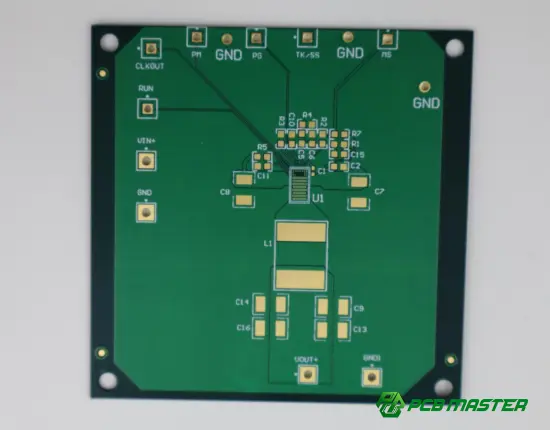
PCB for EV DC/DC converter has high current, high voltage, fast switching signals, limited space, tough automotive reliability requirements. These factors have a direct impact on the efficiency, safety and service life of the converter.
Automotive DC/DC converter PCBs have to operate in much more severe environment than normal electronic PCBs. The PCB has to do much more than just connect components, it has to control power flow, mitigate electrical losses, control heat and maintain stable performance over thousands of hours of vehicle operation.
Supporting high-current power delivery
The EV DC/DC converter PCB needs to be able to transfer large amount of electrical power with minimum energy loss . So the PCB has to have a good current carrying capability.
The DC/DC converter controls power from the high-voltage battery system. Hence the PCB has to be able to handle high current flow through power traces, copper layers and connection points. The additional resistance causes voltage drops , energy loss and heat-up when the PCB design is not capable for the current .
Some PCB design considerations for high current power delivery are as follows:
- Thicker copper layers: Heavy copper PCB designs can carry higher current compared with standard copper thickness.
- Wider traces: Larger trace widths reduce resistance and improve current capacity.
- Shorter current paths: Shorter routes reduce power loss and parasitic effects.
- Optimized copper planes: Large copper areas help distribute current more evenly.
For example, a high power EV DC/DC converter feeding a 48V electrics system will require much thicker copper and optimized power routing than a low power automotive control PCB. Good current handling capability also means avoiding early PCB failure and efficiency.
Maintaining high-voltage electrical isolation
For safety reasons , PCBs used in EV DC/DC converters need to provide reliable high voltage isolation from low voltage control circuits .
The EV battery systems are generally working in the 400V-800V range and the insulation and electrical isolation requirements are high. The PCB must be protected against accidental electrical breakdown which may damage components or create a safety hazard.
Critical design considerations for isolation include:
- Creepage distance: The surface distance between two conductive areas.
- Clearance distance: The air gap between conductive parts.
- Insulation materials: PCB materials must withstand high electrical stress.
- Layer separation: High-voltage and low-voltage circuits require careful stack-up planning.
For instance, the power section connected to an EV battery shall not be placed too close to the low voltage control circuit. A good PCB layout will provide a safe barrier between these areas but will allow for good communication of signals.
The new 800V EV DC/DC converter PCB designs bring with them a need for high voltage isolation. This will be because the electrical safety requirements will be more stringent .
Handling high-frequency switching
EV DC / DC converter PCB has to process high-speed switchings and control electrical noise for better efficiency.
Today, DC/DC converters use high-frequency switching devices like MOSFETs and SiC MOSFETs to efficiently convert power. But fast switching also has some negative effects like voltage spikes, electromagnetic interference (EMI) and signal distortion.
The high frequency switching pcb design main points are as follows:
- Reducing switching loop area: Smaller loops reduce unwanted inductance.
- Optimizing component placement: Power components should be positioned closely together.
- Controlling return paths: Proper current return paths reduce noise.
- Using suitable PCB materials: Low-loss materials may improve high-frequency performance.
SiC based converters can switch faster than traditional silicon devices, so there is more efficiency, but also more challenges in PCB design. PCB design needs to be done carefully to control the switching noise and ensure reliable operation.
Achieving compact size and high power density
Electric Vehicle DC/DC converter PCBs need to pack more power into a smaller space. EVs have very tight size and weight constraints.
Automotive designers are racing to miniaturize electronic modules in the quest to make vehicles more efficient and easier to integrate. We must increase the power density of the DC/DC converter PCBs without sacrificing reliability.
The main design approaches are:
- Multi-layer PCB structures: More layers allow better power distribution in a smaller area.
- High-density component placement: Smaller components help reduce board size.
- Advanced PCB technologies:HDI PCB designs may support compact electronic assemblies.
- Integrated thermal solutions: Space-saving designs must still manage heat effectively.
A next generation EV may require a smaller DC/DC converter to fit into a limited amount of installation space, but still deliver the same or perhaps even larger power output. This requires careful optimisation of PCB layout, materials and component choice.
Meeting automotive reliability requirements
Printed circuit boards in EV DC/DC converters have to be reliable under vibration, thermal cycling and the long life of the vehicle.
Automotive electronic products must operate for many years in harsh environments and high reliability. The power electronics of EVs must: Not like consumer electronics Survive conditions such as:
- Wide temperature ranges
- Mechanical vibration and shock
- Humidity and contamination
- Continuous electrical stress
Automotive grade reliability often requires PCB designs to:
- High-quality PCB materials
- Reliable solder connections
- Robust copper structures
- Strict manufacturing controls
- Comprehensive testing procedures
For example, a DC/DC converter for an EV near the battery pack can experience many temperature cycles when charging and driving. Good PCB design helps to prevent problems such as cracking copper, fatigue of solder and electrical failure.
Automotive reliability requirements guarantee that the DC/DC converter will deliver stable power for the lifetime of the vehicle.
How Should You Select PCB Materials and Stack-Up for an EV DC/DC Converter?
The choice of the right PCB materials and stack-up is the foundation of a reliable EV DC/DC converter PCB. That’s where the choices come in and how the board handles current, voltage stress, heat, signal performance and long-term automotive operation.
Engineers need to define the structure of the board before laying out the PCB including the substrate material, the arrangement of layers, the thickness of copper and the insulation design. A well designed PCB stack-up helps to establish stable power paths, helps to improve thermal performance and reduces the potential failures during vehicle operation.
Choosing the right PCB substrate material
The right electrical, thermal and mechanical properties of the PCB substrate material are mandatory to meet the EV DC/DC converter power requirements.
FR-4 is the most common material for automotive DC/DC converter PCBs but not all FR-4 material is created equal. Grades are often specified higher for high power EV applications, where higher thermal stability and reliability are needed.
Important properties of materials are:
- High glass transition temperature (Tg): Helps the PCB maintain mechanical strength under high operating temperatures.
- Low moisture absorption: Improves reliability in humid automotive environments.
- Stable dielectric properties: Supports consistent electrical performance.
- Good thermal resistance: Helps manage heat generated by power components.
For example, a standard FR-4 can be used for designing a low power automotive control board, while a high power EV DC/DC converter PCB may require high-Tg FR-4 for better thermal reliability. Choosing the right PCB material avoids issues such as delamination, warping and degradation of performance over the life of the operation.
Selecting the optimal PCB layer count
You need enough PCB layers to route power, signals, isolate circuits and dissipate heat, but not so many that it gets complicated.
The PCBs for EV DC/DC converters are mostly multilayer, as single or double layer PCBs are not able to handle the high current and complex control signals efficiently, most of the time.
A suitable stack-up of layers could include:
- Outer layers for component connections and routing
- Internal copper planes for power and ground distribution
- Dedicated signal layers for control circuits
- Isolation layers between high-voltage and low-voltage sections
For instance a simple low power converter may have a 4 layer PCB. But a higher power automotive DC/DC converter may have 6 or 8 or even more layers to keep the power and control circuits well separated.
But more layers do not always mean better performance. The number of layers has to be selected based on actual electrical requirements, power density, manufacturing capability and cost constraints.
Determining the appropriate copper thickness
The thickness of the copper on an EV DC/DC converter PCB will determine how much current can safely pass through it and how well it can spread the heat.
While typical PCBs use thinner copper layers, power electronics applications need thicker copper to reduce electrical resistance and temperature rise.
Typical copper thickness considerations are:
- Higher current → thicker copper required
- Longer current paths → greater copper capacity needed
- Higher power density → better heat spreading required
For high current automotive power applications, heavy copper PCBs like 2 oz, 3 oz or more copper weights are often considered.
A dc/dc converter, for example, that handles several hundred watts of power will require more robust current paths than a small electronic control module. Thicker copper can reduce power loss and improve the PCB’s reliability (under continuous use).
Designing effective power and ground planes
Good power and ground plane in an EV DC / DC converter PCB gives stable current distribution and less electrical noise .
Ground and power planes are used to control unwanted electrical noise and to provide stable voltage references . Power planes provide low resistance paths for high current flow.
A good power and ground structure should:
- Provide short current return paths
- Reduce voltage fluctuations
- Improve electromagnetic compatibility (EMC)
- Support better heat distribution
For example, by careful design of the plane, interference from the microcontrollers, sensors and communication circuits can be prevented by separating the noisy switching power areas from the sensitive control circuits.
Internal copper planes are commonly used in high power EV DC/DC converter PCB design to carry large current and leave the external routing area for components and control signals.
Planning dielectric thickness and electrical isolation
You make the dielectric thicker to get electrical insulation, or to control the signal behaviour, or to get a safe distance between different voltage levels.
The dielectric layers between copper layers have to be carefully designed, as EV DC/DC converters work with high voltage battery systems that can be 400V or 800V.
Important considerations are:
- Insulation thickness between high-voltage layers
- Controlled impedance requirements
- Voltage withstand capability
- Creepage and clearance requirements
The thicker dielectric layer can improve the electrical isolation and the thinner one can be used to reduce the size of the PCB and improve the coupling of the signals. These factors have to be balanced by the engineers with the application needs.
For example, an 800V EV system requires more detailed insulation design to avoid electrical breakdown and maintain passenger safety than a conventional 12V automotive circuit.
Balancing electrical, thermal, and mechanical performance
A good PCB design for an EV DC/DC converter must optimize electrical performance, thermal management and mechanical reliability, not just one parameter.
Each PCB design choice influences multiple performance parameters:
- A thicker copper layer improves current capacity but may increase manufacturing complexity.
- More PCB layers improve routing flexibility but increase cost and production difficulty.
- Advanced materials improve reliability but may require stricter manufacturing processes.
These factors are normally considered together by the engineers during the stack-up design phase.
For example, an EV DC/DC converter PCB used around the battery pack should provide good electrical insulation, good thermal performance and mechanical robustness against the vibration. All three requirements are achievable with a proper choice of material and stack-up, and still be manufacturable.
Thus, the choice of PCB material and stack-up design are not simply manufacturing choices, but engineering decisions that can determine successful production, efficiency, and reliability of the final converter.
What PCB Layout Practices Improve Electrical Performance?
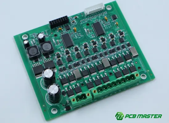
Good PCB layout can help the electrical performance of an EV DC/DC converter, reducing power losses, controlling switching noise, improving signal stability and ensuring efficient current flow.
The EV DC / DC converter PCB unlike a normal electronic board operates with high voltage, high current and fast switching signals at the same time. Therefore, the PCB layout has a great impact on the connection of the components as well as the converter efficiency, electromagnetic compatibility (EMC) and long-term reliability.
The layout design is optimized to minimize the critical current path, to control the undesired electrical effects and to provide a clear separation between the power and control circuits.
Optimizing component placement
Place components to minimize the length of electrical connections and provide an efficient path for current flow.
The first step in designing an EV DC/DC converter PCB layout is to group the components according to their electrical functions. The power components, control components and the sensing circuits should be arranged based on their roles in the circuit.
Placement is based on the following core principles:
- Placing switching devices close to related power components
- Keeping high-current components physically close together
- Positioning control circuits away from noisy power areas
- Placing sensors near the circuits they monitor
For example, all the MOSFETs, inductors and capacitors in the power conversion stage should be placed close to each other to minimize the unnecessary connection length. At the same time, keep the microcontroller and communication circuits away from high noise switching areas.
Proper component placement can minimize parasitic effects and enhance circuit stability, laying a strong foundation for the overall design of the EV DC/DC converter PCB.
Minimizing high-current loop inductance
Reduce the inductance of the high current loop, then reduce voltage spikes, switching losses and electromagnetic interference.
In DC to DC conversion the switching loops carry high speed current. These loops will have some parasitic inductance which can cause unwanted voltage spikes when the current changes quickly.
PCB designers can do the following to minimize loop inductance:
- Keep high-current loops as small as possible
- Place switching components close together
- Use short and direct copper connections
- Avoid unnecessary routing turns
For example, in a synchronous buck converter, a very critical location is the loop of the MOSFETs, input capacitors and inductor. A large loop can lead to larger electrical noise while a small loop results in improved switching efficiency and reliability.
One of the most critical PCB layout practices for high performance EV DC/DC converter designs is to reduce high current loop inductance.
Routing high-current traces efficiently
High current traces need to be wide , thick and routed efficiently to safely carry power and minimize loss .
The power traces on a PCB of an EV DC/DC converter carry far more current than standard automotive electronic boards. Poor trace design can create resistance, generate heat and lower converter efficiency.
Things to bear in mind when routing high currents:
- Using wider traces for higher current paths
- Applying thicker copper layers when required
- Avoiding narrow sections and sharp corners
- Keeping high-current routes short
For example, a 48V vehicle system using a DC/DC converter may have to use heavy copper PCB technology to be able to handle the continuous current safely. A wider copper trace will reduce the voltage drop and improve energy efficiency.
In addition, design of high current traces should consider manufacturing capability so that the PCB can be consistently manufactured in mass production.
Designing low-impedance return current paths
Low impedance return path maintains voltage levels and reduces electrical noise.
Current needs a complete path back to source from return point. If the return path has high impedance or the routing distance is too long, there can be voltage fluctuation and electromagnetic interference can rise.
The good return current path design is:
- Using continuous ground planes
- Avoiding unnecessary gaps in reference planes
- Keeping return paths close to signal paths
- Reducing current loop areas
Stable reference planes are needed in an EV DC/DC converter for high speed control signals. Poor ground return path can lead to noise in the control signals and upsetting the converter operation.
A good return path design also enhances signal integrity and makes reliable communication between the power stage and the control circuits possible.
Separating power, control, and signal circuits
The various parts of the circuit are separated so that power switching noise does not couple into sensitive control and communication signals .
A typical EV DC/DC converter PCB has three major areas as follows:
- Power circuits: Handle high voltage and high current.
- Control circuits: Manage switching and converter operation.
Signal circuits: Process sensing and communication information.
These areas should be located physically to avoid interference. High power switching areas should be separated from sensitive analogue sensing circuits or communication interface.
For example, current sensors and voltage feedback circuits require clean signals to accurately control the converter. Routing near noisy switching nodes can cause measurement errors.
Proper circuit separation can enhance the control accuracy, EMC performance and stability of converter.
Reducing parasitic inductance and voltage spikes
Avoid parasitic inductance to prevent unexpected voltage spikes and improve reliability of switching devices .
Parasitic inductance is the unwanted inductance of PCB traces, vias and component connections. It 's small , but can be important when you have fast switching of high currents .
Techniques for parasitic inductance reduction in PCB layouts include:
- Shortening component connections
- Reducing unnecessary vias
- Keeping switching paths compact
- Using optimized copper structures
The fast turn-off of a MOSFET can cause voltage overshoot due to energy stored in parasitic inductance. Such voltage transients stress components and reduce the life time of the components.
Careful control of the PCB geometry and current paths allows designers to improve the switching performance, decrease the electrical stress and increase the reliability of PCBs for EV DC/DC converters.
How Can You Improve Thermal Performance in an EV DC/DC Converter PCB?
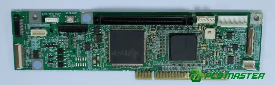
Improve thermal performance of an EV DC/DC converter PCB. Identify heat sources, design copper structures efficiently, use thermal vias, optimize heat distribution and properly connect PCB with external cooling solutions.
Thermal management is an important consideration in the EV DC/DC converter PCB design since the system produces a large amount of heat during the power conversion process. A high temperature may cause a decrease in the component lifetime, an increase in electrical losses and reliability problems. A proper thermal approach can improve the stability of the converter in steady load and in harsh automotive conditions.
Identifying major heat-generating components
The first step in the thermal design is to identify the components that generate the most heat and need the most efficient cooling paths.
Heat in an EV DC / DC converter PCB is mainly produced by components that switch current fast or handle high power. The main heat-producing parts are usually:
- Power MOSFETs or SiC MOSFETs: Generate switching losses during high-frequency operation.
- Inductors and transformers: Produce heat due to current flow and magnetic losses.
- Diodes or rectifiers: Create heat from voltage drops during operation.
- Power resistors: Dissipate energy as heat.
Thermal analysis is usually performed by engineers in the design phase to understand temperature distribution and potential hot spots.
For example, in an 800V EV platform, a high power DC/DC converter could have a lot of heat concentrated around the switching devices. Improper management of these areas may cause local overheating which reduces the reliability of the components and the lifetime of the converter.
Knowing where the heat is provides designers the opportunity to develop specific cooling solutions instead of applying the same solution to the entire PCB.
Increasing heat dissipation with copper planes
Big chunky bits of copper help thermal performance by spreading heat away from hot components .
Copper is a good conductor of heat, and this is why PCB designers use internal and external layers of copper to spread the heat effectively. Electrical and thermal functions of copper planes in an EV DC/DC converter PCB are designed.
Thermal design commonly uses the following techniques:
- Increasing copper thickness
- Adding larger copper areas around power components
- Using internal copper planes for heat spreading
- Connecting heat sources to wider copper regions
For example a heavy copper PCB with thicker copper layers can carry more current and better dissipate heat than a standard PCB.
But copper design is a delicate dance. Too many areas of copper can affect impedance control, manufacturing processes or PCB weight. Therefore copper planes should be optimized for the actual requirements, the thermal conditions and the production capability.
Using thermal vias effectively
Thermal vias are used to transfer heat from the component side of the PCB to internal or bottom copper layers.
A thermal via is a small plated hole that passes heat through the PCB. Usually these vias are placed under or near high power components to pull heat from hot spots.
Good thermal via design includes:
- Using multiple vias instead of a single via
- Placing vias directly under heat-generating components
- Connecting vias to larger copper areas
- Considering via size and manufacturing limitations
Switching power MOSFETs in a DC/DC converter in an electric vehicle can generate a lot of heat. A good thermal via array will help to transfer the heat from the component pads to the inner copper planes, which will reduce the operating temperature.
Thermal vias are particularly useful when a PCB cannot be directly placed on a heatsink, or when there is not much space for cooling due to component density.
Optimizing heat spreading across the PCB
Optimized heat spreading spreads thermal energy over a larger area of the PCB to avoid local hotspots.
The PCB of the DC/DC converter should not only dissipate heat of individual components, but also prevent uneven temperature distribution. Large temperature differentials everywhere cause mechanical stress and affect long term reliability.
The methods of heat conduction are:
- Placing heat-generating components with enough spacing
- Using continuous copper areas
- Balancing copper distribution between layers
- Avoiding concentrated heat in one PCB region
For example, if you have several high power parts close to each other, you can create a thermal hot spot even if each part is within its own temperature limit. Good layout has heat sources at various locations and more heat paths.
Good heat spreading improves reliability by reducing thermal stress on solder joints, PCB materials and electronic components.
Integrating the PCB with heatsinks and cooling systems
PCB can be used with external cooling methods for heat removal from high power EV DC/DC converter systems.
In higher power automotive applications, thermal design may be more than a PCB level issue. Often additional solutions are needed to cool the converter assembly such as:
- Aluminum heatsinks
- Thermal interface materials (TIMs)
- Liquid cooling systems
- Vehicle cooling loops
In PCB design, we need to consider the heat flow from the components to these external cooling structures. Correct mechanical alignment, thermal contact areas, and mounting methods are important factors.
For example, an EV DC/DC converter close to the battery system might be housed in a metal enclosure that is connected to the vehicle cooling system. The PCB, power components and enclosure must form a complete thermal system acting in concert.
Integrating PCB thermal design with mechanical cooling solutions enables engineers to achieve stable operating temperatures, increase efficiency and extend the life of automotive power electronics.
How Can You Reduce EMI and Ensure EMC Compliance?
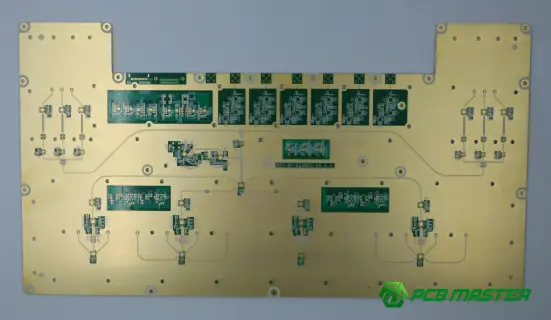
On an EV DC/DC converter PCB, EMI can be reduced by controlling the noise source, optimizing the filter and grounding, using shielding, and following EMC-oriented PCB layout practices.
A DC/DC converter switches electrical energy very fast and therefore inherently creates electromagnetic noise. This noise can affect nearby systems such as sensors, communication modules and vehicle control units, if not properly controlled. Thus, EMI (Electromagnetic Interference) control and EMC (Electromagnetic Compatibility) design are important design considerations for an automotive DC/DC converter PCB.
A good design will allow the converter to run efficiently without disturbing the other electronic systems on the vehicle.
Common EMI sources in EV DC/DC converters
The main sources of EMI in EV DC/DC converters are: high frequency switching, fast current changing and unwanted electrical paths.
The electromagnetic noise is generated by the switching operation of the power devices such as MOSFET and SiC MOSFET. Such devices switch very fast, resulting in voltage and current changes with high frequency.
Common sources of EMI are:
- Switching nodes: Fast voltage transitions generate radiated noise.
- High-current loops: Rapid current changes create magnetic fields.
- Parasitic inductance and capacitance: Unwanted electrical effects increase noise levels.
- Poor grounding paths: Incorrect return paths allow noise to spread.
For instance, SiC MOSFETs can lead to higher efficiency in an EV DC/DC converter because of its faster switching speed. The downside to this is the faster you switch the more EMI problems you will have. So, a good PCB design is important.
Early identification of noise sources enables engineers to implement specific solutions instead of late-stage, unnecessary design changes.
Optimizing filter placement
Proper placement of filters reduces conducted noise by preventing unwanted signals from entering or leaving the DC/DC converter.
Filters permit normal power flow and reject high frequency noise. But the filter parts need to be placed the right way around on the PCB for them to work correctly.
Best Practices for Filter Placement:
- Positioning input filters close to power entry points
- Keeping filter paths short and direct
- Separating noisy switching areas from filter circuits
- Placing capacitors close to switching components
For example if an input capacitor is located too far from the switching devices it may not be able to suppress high frequency noise sufficiently due to the added inductance of the extra trace length.
Filter design and placement should be considered together on an EV DC/DC converter PCB. Even a well designed filter will not give the desired EMI reduction if it is badly placed on the PCB.
Designing effective grounding strategies
A good grounding strategy provides a good return path for the current and prevents noise from propagating around the PCB.
One of the most important factors for a performance of the EMC is a design of ground. Bad grounding can lead to unwanted current loops, more noise and communication problems between vehicle systems.
Some best practices for grounding:
- Creating low-impedance return paths
- Keeping high-current return paths short
- Separating noisy power grounds from sensitive signal grounds when needed
- Using proper ground plane structures
Control circuits need a clean ground reference to measure current and voltage. They can have uncontrolled return path, high power switching currents and measurement errors and unstable converter operation can occur.
A good way to reduce the conducted and radiated EMI, and improve the overall reliability of the EV DC/DC converter PCB is to have a proper grounding strategy.
Applying shielding techniques where necessary
Shielding prevents the electromagnetic radiation emitted by high frequency switching circuits from radiating out.
A good PCB layout will take care of most of the EMI problems, but some high power converters for automotive applications may need other shielding techniques.
Common methods of shielding are:
- Using metal enclosures around the converter
- Adding shielding covers over sensitive areas
- Creating controlled grounding connections between shield structures and PCB ground
- Reducing exposed high-noise areas
For example, a DC/DC converter located close to communication modules or sensitive sensors might need better EMI shielding, since electromagnetic noise can degrade system performance.
But shielding should not be the first solution. Adding a shield isn’t always the fix for a bad layout. Good EMC design always starts with the PCB structure, current paths, grounding and filtering before any other shielding is done.
PCB design practices that support EMC compliance testing
The idea of EMC friendly PCB design is to increase the probability of passing the automotive electromagnetic compatibility tests by controlling noise before production.
Automobile electronics are EMC tested so they do not interfere with the other systems in the vehicle. The decisions made early in the PCB design process have a huge impact on the test results.
Some of the important PCB EMC practices are:
- Minimizing high-frequency current loops
- Separating power and sensitive signal areas
- Controlling switching node size
- Maintaining proper grounding structures
- Placing filters and decoupling components correctly
- Reducing unnecessary vias and long traces in noisy areas
For example, if the prototype fails the EMC testing due to too much switching noise, redesigning the PCB layout can be a very time consuming and expensive process. The early EMC design consideration in the PCB design stage of the EV DC/DC converter can shorten the development cycles and improve the mass production readiness.
A PCB designed for EMC requirements is more reliable, easier to certify and more stable in real automotive environment.
What Automotive Standards and Manufacturing Requirements Should You Consider?
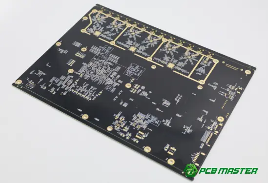
The PCB for the EV DC/DC converter needs to meet the automotive standard, high-voltage safety standard, manufacturing regulation and reliability test requirements to ensure the stable operation during the whole service life of the vehicle.
Unlike consumer electronics, automotive power electronics are expected to work reliably under vibration, temperature variation, electrical stress and lifetime use Therefore, the PCB design and PCB manufacturing process should be considered together from the early development stage to prevent failure in the mass production.
PCB standards for automotive applications
Automotive PCB standards govern the quality, reliability and manufacturing standards required for vehicle electronics.
In general, PCBs for EV DC/DC converters should be designed according to industry standards, which specify PCB material, fabrication quality, assembly processes and inspection methods.
The main standards and requirements are:
- IPC standards: Define PCB manufacturing and assembly quality levels.
- IATF 16949: A key automotive quality management standard for suppliers in the automotive industry.
- AEC-Q requirements: Define reliability expectations for automotive electronic components.
- RoHS compliance: Restricts hazardous substances in electronic products.
For example a manufacturer of DC / DC converter boards for the automotive industry requires consistent process control, traceability and quality inspection in order to meet the reliability requirements of the vehicle manufacturers.
Adherence to automotive standards is more than certification. And the PCB is assured to have stable electrical and mechanical performance for years of vehicle operation.
Creepage and clearance design requirements
The design of creepage and clearance is for preventing electrical breakdown on EV DC/DC converter PCBs and ensuring safe isolation of high voltage circuits.
Most EV battery systems operate at either 400V or 800V, so PCB designs must be very careful about the spacing between conductive areas.
The two notions are of significance:
- Clearance: The shortest distance through air between two conductive parts.
- Creepage: The shortest distance along the PCB surface between two conductive parts.
Good creepage and clearance design can prevent:
- Electrical arcing
- Insulation failure
- Short circuits
- Safety risks
For example, the high-voltage input section attached to an EV battery needs to be physically isolated from low-voltage control circuits. The distances shall be determined by the designers according to the operating voltage, the properties of the materials, the degree of contamination and the safety requirements.
Right isolation design is very important for next generation 800V EV DC/DC converter PCB application.
Design for Manufacturability (DFM) considerations
In other words, DFM enables a reliable, efficient, and consistent mass production of an EV DC/DC converter PCB.
Even an electrically correct PCB design can have problems with manufacturing if the production requirements are ignored. DFM reviews can uncover potential problems before fabrication.
Critical DFM problems include:
- Selecting manufacturable trace widths and spacing
- Designing reliable via structures
- Avoiding unnecessary manufacturing complexity
- Considering PCB assembly processes early
- Ensuring stable production yield
For instance a heavy copper PCB design may carry more current but too much copper thickness changes the etching, plating and manufacturing requirements. The production capability should be balanced with the electrical performance .
Early collaboration between PCB designers and manufacturers in DFM helps reduce redesign cycles, increase production efficiency and ensure consistent quality in volume production of automotive parts.
PCB assembly and solderability requirements
The PCB assembly and solderability requirements specify how electronic components shall be securely attached and maintain reliable connections during vehicle operation.
In the PCBs of EV DC/DC converters, the power parts are often subjected to constant electrical and thermal stress. Therefore the solder joints must be mechanically and electrically strong.
Key Assembly considerations are:
- Suitable surface finish selection
- Proper solder paste application
- Accurate component placement
- Reliable solder joint formation
- Compatibility with automated SMT processes
Common automotive PCB finishes are:
- ENIG (Electroless Nickel Immersion Gold)
- OSP (Organic Solderability Preservative)
Low quality solder on a high current power component can create high resistance and heat generation which will eventually lead to the failure of the converter.
We have developed a robust assembly process to ensure the EV DC/DC converter PCB operates uniformly in presence of vibration, temperature cycling and long term operation.
Inspection and reliability testing before production
Prior to mass production, inspection and reliability testing must be performed to ensure the EV DC/DC converter PCB meets electrical, mechanical and quality requirements.
In the automotive PCB manufacturing, there are several times of testing that prevent field failure.
Common methods of inspection and testing include:
- Automated Optical Inspection (AOI): Detects surface defects and component placement issues.
- Electrical testing: Verifies circuit continuity and insulation performance.
- X-ray inspection: Checks hidden solder joints and internal structures.
- Thermal testing: Evaluates temperature performance under operating conditions.
- Reliability testing: Simulates long-term automotive environments.
Prototype PCBs for the DC/DC converter may be temperature cycled, vibration and electrical stress tested before approval for vehicle production.
The rigorous validation and review process allows manufacturers to catch problems early, improve reliability in manufacturing and deliver quality EV DC/DC converter PCBs for the automotive industry.
What Common EV DC/DC Converter PCB Design Mistakes Should You Avoid?
The most common mistakes in EV DC/DC converter PCB design come from wrong material selection, poor stack-up planning, bad power routing, bad thermal design, poor EMI control, and ignoring manufacturing requirements.
The PCB for a DC/DC converter has to satisfy the demands of electrical performance, thermal reliability, safety and manufacturability. But if the design is not thought through from the start it may work in a simulation or prototype test but not in mass production.
In real-world automotive applications, avoiding these common design mistakes will reduce development costs, improve converter efficiency and enhance long-term reliability.
Choosing unsuitable PCB materials or copper thickness
An EV DC/DC converter PCB made with the wrong material or copper weight can have limitations in current capability, thermal performance and service life.
The PCB's resistance to electrical, thermal and mechanical stress is directly determined by the choice of material. If a standard PCB material is used in a high power application it may result in excessive heat, degradation of materials or lower reliability.
The usual mistakes are:\
- Using low-performance materials for high-temperature environments
- Selecting insufficient copper thickness for high current loads
- Ignoring thermal and mechanical requirements during material selection
For example, high power EV DC/DC converters may need high-Tg FR-4 and thicker copper layers for continuous current operation. If the copper thickness is not enough in a PCB, then it will result in higher resistance, power loss and heating.
When choosing the right material and copper consideration should be given to voltage, current, working temperature and expected life time of the vehicle.
Designing an inefficient PCB stack-up
Bad or incorrect PCB stack-up can cause unstable power delivery, poor electrical isolation, and more noise problems.
The PCB stack-up specifies the layout of the internal layers on the board, such as power layers, ground layers, signal layers and insulation layers. Structure is bad. Difficult to control current paths and maintain high signal quality.
Common errors in stack-up are:
- Placing power and ground layers incorrectly
- Insufficient isolation between high-voltage and low-voltage circuits
- Using unnecessary layers without improving performance
- Failing to consider impedance and current distribution
For example, an EV DC/DC converter PCB operating at 800 V must have internal layers designed with careful consideration for safe electrical separation. Bad layer stacking increases the possibility of insulation failure or EMI.
Good stack-up means stable power distribution, better EMC performance and easier PCB production.
Creating excessive switching loop areas
Big switching loops in EV DC/DC converter PCBs increase parasitic inductance, voltage spikes and electromagnetic interference.
Power converters with fast switching operation can be operated with high efficiency. However, each switching loop has unwanted electrical effects when the current changes quickly.
A large switching loop can produce:
- Higher voltage overshoot
- Increased switching losses
- More EMI emissions
- Greater stress on power components
For instance, if the MOSFET, input capacitor and inductor are located too far apart, the current path is longer and adds inductance. This may have an impact on component reliability and decrease the converter efficiency.
In PCB layout process, designers need to keep the critical switching paths short, place the related components close and optimize the current loops to reduce the problem.
Underestimating thermal challenges
Poor thermal design in EV DC/DC converters can lead to overheating, inefficiency and early failure of components.
Power conversion in general and especially in high current components like switching devices and inductors is inherently a source of heat. The heat transfer PCB may not be good enough to make temperature too high.
Common thermal design errors are:
- Ignoring heat generated by power components
- Using insufficient copper areas
- Poor placement of thermal vias
- Not considering external cooling solutions
For example, a converter may pass initial functional testing, but fail in long term operation due to repeated thermal cycling damaging solder joints or electronic components .
A good thermal design should be started at the PCB planning stage with copper distribution, thermal vias, component placement and mechanical cooling integration.
Overlooking EMI and grounding issues
Poor EMI and grounding design can allow electrical noise to enter that can degrade converter performance and communication with other vehicle systems .
The high speed switching circuits in EV DC/DC converters are inherently generating electromagnetic noise. If not handled properly, this noise can interfere with sensors, controllers and communication networks.
Common errors include:
- Creating uncontrolled current return paths
- Mixing noisy power areas with sensitive signal circuits
- Poor placement of filter components
- Ignoring grounding strategy
Unstable groundings can cause noise to the voltage feedback signals, which may lead to inaccurate measurement and affect the control performance of the converter.
Designers need to consider EMI control from the start, not as a cure after test failures. Designers should separate power areas from signal areas and provide clear return paths for better EMC performance.
Ignoring manufacturability during the design stage
If you don’t consider manufacturing requirements you will probably have more manufacturing problems, lower yield and higher redesign costs.
A PCB design must not only function electrically, it must also be buildable. Some designs may look good in a prototype, but difficult or costly in automotive mass production.
Common errors in manufacturability are:
- Designing features beyond manufacturing capabilities
- Ignoring PCB fabrication limitations
- Using difficult-to-produce via structures
- Not considering SMT assembly requirements
For example, a heavy copper PCB design may improve the electrical performance, but poor planning may cause problems during etching, plating and soldering.
Early DFM reviews help to identify these problems prior to production. Including a PCB manufacturer in the design process speeds up the development time, increases consistency in production and allows for production at automotive scale.
By avoiding these common mistakes in EV DC/DC converter PCB design, engineers can design boards that are the right balance of power performance, thermal reliability, EMC compliance and manufacturability. This is necessary to develop solutions for automotive grade PCBs that can operate safely throughout the life of the car.
Conclusion
PCB design of an EV DC/DC converter is a delicate balance of electrical, thermal, EMC and manufacturing reliability concerns. Every decision from materials selection, stack-up planning and layout optimization to production test can have a direct impact on the converter efficiency and service life.
So it’s important to find a PCB partner with the experience to translate a good design concept into a production-ready solution. PCBMASTER can help engineers design rugged EV DC/DC converter PCB solutions that meet the demanding parameters of today’s electric vehicles by drawing on its knowledge in automotive PCB production, advanced materials, high current designs, and rigorous quality control processes.
With EV platforms continuing to evolve to higher voltage systems with more power density, optimized PCB design will continue to be a key factor in achieving safer, more efficient and more reliable automotive power electronics.
FAQs
What PCB layer count is commonly used for EV DC/DC converter PCBs?
The PCBs of the EV DC/DC converters are generally 4, 6 or 8 layer boards depending on the power level, voltage requirements and the complexity of the layout.
Lower power designs can use 4 layer boards. High power automotive converters need better power distribution, electrical isolation, EMI control and signal management and hence 6 or 8 layer PCBs are often used.
The optimum number of layers is a function of current carrying capability, voltage rating, thermal requirements and manufacturing considerations.
When should you use heavy copper PCBs in EV DC/DC converter designs?
When you want a converter that can handle high current and has better thermal performance, you use heavy copper PCBs.
Thicker copper layers (2oz or greater) reduce resistance, reduce power loss, and improve heat spreading.
They are often used in high power EV DC/DC converters where continuous current loading is a greater electrical and thermal challenge.
How are EV DC/DC converter PCBs different from onboard charger (OBC) PCBs?
DC / DC converter PCBs that step down battery voltage to power vehicle systems. OBC PCB converts AC power from outside to DC power to charge the battery.
DC/DC converter PCB goals:
- High-current output
- Voltage conversion efficiency
- Compact design
OBC PCBs have to perform some other functions like AC input, power factor correction and charging control.
The functions are different. So are their PCB structure & components and testing requirements .
Which PCB surface finish is best for automotive DC/DC converter applications?
ENIG is widely used on automotive DC/DC converter PCB’s because it is reliable, flat and solderable.
ENIG is also used when cost efficiency is important, but it offers greater long-term stability for demanding automotive applications.
Finally, the choice depends on the assembly process, the requirements as to the reliability and the conditions of production.
How can you choose the right PCB manufacturer for an automotive DC/DC converter project?
Pick a manufacturer with automotive experience, advanced PCB capabilities and solid quality control.
The important factors are:
- Heavy copper and multi-layer PCB capability
- High-voltage isolation experience
- Automotive quality certifications
- DFM and engineering support
- Reliable testing processes
A good PCB manufacturer can help you optimize materials, stack-up and production processes for improved reliability and manufacturability of EV DC/DC converter PCBs.
About the Author

Carol Luo
PCB Design EngineerI'm Carol, a PCB Engineer at PCBMASTER with experience in PCB design and manufacturing engineering since 2018. I focus on translating engineering requirements into reliable PCB solutions, with expertise in stack-up design, material selection, and design-for-manufacturing (DFM). I share practical engineering insights from real-world PCB design and production experience.
Visit Carol Luo's Profile