


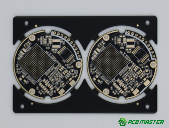
Backdrilling in High-Speed PCBs: A Complete Guide to Signal Integrity
As digital circuits continue to push toward higher frequencies and faster data rates, high-speed, multi-layer PCBs are facing increasingly demanding challenges. Even minor imperfections in the board can affect signal quality, leading to reflections, delays, and data errors. One common issue in these designs is the presence of leftover copper inside plated through holes (PTHs). While seemingly insignificant, these excess copper segments can severely disrupt high-speed signal transmission.
As a result, removing such redundant copper has become an essential step in modern PCB manufacturing. Proper management of these features ensures that signals travel cleanly between layers, reducing losses and improving the overall performance of the board. At the same time, effectively controlling this process requires careful attention to manufacturing tolerances, material properties, and the PCB’s layer structure.
So how can backdrilling be properly implemented in PCB manufacturing? PCBMASTER, a seasoned PCB and PCBA supplier, has accumulated extensive experience in this area. This article will draw on PCBMASTER’s practical expertise and industry knowledge to provide an in-depth look at what backdrilling is, why this advanced process is critical for high-speed PCB design, and how engineers can determine appropriate process parameters and implement best practices for testing and verification. Our goal is to provide actionable guidance for designers striving to achieve reliable signal integrity and exceptional board performance.
What is PCB Back Drill (Back Drill) Technology?
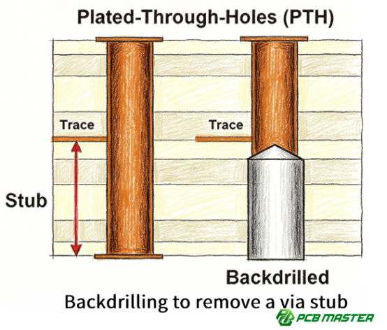
PCB back drilling is a manufacturing technique used to remove unused copper in plated through holes (PTH), also known as stubs, in multi-layer printed circuit boards (PCBs). This helps improve high-speed signal integrity by reducing signal reflections and transmission loss.
Definition and Basic Concept of Back Drill
Back drilling is designed to eliminate the unused copper section inside a PTH hole, commonly referred to as a stub. These stubs act like tiny antennas, causing signal reflection, scattering, and delay in high-frequency circuits.
In simpler terms, imagine a water pipe where part of the pipe goes beyond the faucet. Water (or signals) doesn’t flow efficiently past the faucet, and leftover sections can cause turbulence. In PCBs, these leftover copper stubs can distort signals. Back drilling removes the “extra pipe” so the signal can travel cleanly.
Back Drill Manufacturing Process
The back drill process is a two-step method:
1. Initial through-hole drilling and plating: The PCB is drilled like a standard via hole and plated with copper to create the electrical connection between layers. This is the usual PTH process.
2. Secondary drilling with depth control: Using precision drilling machines, the unused copper stub is drilled out. The drill depth is carefully controlled to remove only the unnecessary section while keeping the necessary electrical connection intact.
A practical example: For one of PCBMASTER’s 16-layer PCBs, a via connecting layers 2–6 had a stub extending to layer 16. Back drilling removed the stub from layers 7–16 while keeping the electrical connection between layers 2–6 intact.
PCBMASTER Back Drill Process Advantages
PCBMASTER uses advanced back drilling techniques to enhance signal performance and manufacturing precision:
l Precise drill depth control: Our machines maintain a tolerance of 4–8 mils, ensuring minimal stub residuals without cutting through active layers.
l Improved high-frequency signal integrity: By removing unwanted copper, back drilling reduces signal reflections, lowers transmission loss, and supports high-speed digital designs.
Example: In a PCBMASTER project, a 16-layer high-speed board carrying a 10 Gbps signal had PTH stubs beyond the intended layers. After back drilling, signal tests showed a 20% reduction in reflections compared to a non-back-drilled board, improving signal quality and confirming the effectiveness of precise stub removal.
Why Must High-Speed PCB Designs Consider Back Drilling?
Back drilling is essential in high-speed PCB design because unused copper stubs in vias can distort signals, causing reflections, delay, and signal loss. Removing these stubs ensures cleaner, faster signal transmission and reduces high-frequency design issues.
How Do Stubs Affect High-Speed Signals?
Unused copper sections, or stubs, act like tiny antennas inside the PCB. They cause signal reflection, scattering, and delay, which degrade high-speed data transmission. Each stub can create small echoes that interfere with the main signal, especially at multi-gigabit frequencies.
For example, in PCBMASTER’s testing of a 10 Gbps digital board, stubs extending beyond the intended via layers created measurable reflections. Reducing the stub through back drilling improved the signal’s clarity. Engineers often quantify the impact: every 1 mil of stub depth can cause about 0.25% additional signal loss. This makes stub removal critical for high-frequency, multi-layer PCBs.
What Challenges Do High-Frequency, High-Speed PCB Designs Face?
High-speed PCB designs face two major technical challenges:
l Signal Integrity (SI) issues: At high frequencies, signals are sensitive to even small impedance changes. Unremoved stubs create discontinuities that cause reflections and timing errors.
l Electromagnetic Compatibility (EMC) issues: Stubs can radiate electromagnetic noise, interfering with nearby traces and components. High-power or fast-switching signals amplify this problem.
A real example from PCBMASTER: A 12-layer PCB carrying high-speed memory interface signals (6–8 Gbps) showed intermittent errors. After applying back drilling to remove stubs, signal integrity improved, and electromagnetic interference was reduced, enabling reliable data transmission.
How Does PCBMASTER Optimize Back Drilling for High-Speed Designs?
PCBMASTER tailors back drilling to signal frequency, layer structure, and signal type:
l Frequency-based selection: Higher-frequency signals require shorter stubs, while low-frequency signals may tolerate longer residuals.
l Signal type consideration: Differential pairs, clocks, and high-speed serial interfaces are prioritized for stub removal to maintain timing and minimize reflections.
l Layer planning: Engineers specify back drilling start and stop layers for each via to avoid cutting functional connections while removing unnecessary copper.
For instance, on a 16-layer high-speed board transmitting 10 Gbps PCIe signals, PCBMASTER calculated the maximum stub length allowed per via and applied precise back drilling. Testing confirmed reduced signal reflections and consistent data integrity across all layers.
How Are Back Drill Hole Parameters Determined and Controlled?
Back drill parameters are carefully planned to remove unwanted via stubs while preserving essential electrical connections. Key considerations include drill depth, operational layers, hole size, safety spacing, and residual stub control. Proper control ensures high-speed signal integrity and reliable PCB performance.
How Is Back Drill Depth and Operational Layer Controlled?
Back drill depth must be carefully set to remove only the unnecessary stub copper while keeping the via connection intact.
PCBMASTER specifies the start and stop layers for each back-drilled via based on the signal path. For example, a via connecting layers 3–7 may have a stub extending to layer 14. The back drill removes the copper from layers 8–14, leaving the connection intact between 3–7.
Tolerance considerations: Drill depth is affected by both machine precision and PCB thickness variations. PCBMASTER controls these factors to maintain a residual stub within 4–8 mils, ensuring no open circuits while minimizing signal reflections. This approach guarantees reliable high-speed performance across multi-layer boards.
What Are the Hole Size and Safety Spacing Requirements?
Back drill hole diameter and spacing are critical to prevent damage and maintain signal integrity.
l Hole size: Back drill holes are typically about 10 mils larger than the original via to ensure complete stub removal.
l Safety spacing: Adequate clearance prevents interference with nearby traces, other vias, or pads. PCBMASTER follows precise rules, such as 20 mils from adjacent inner-layer traces, 10 mils between back drill holes, and 15–20 mils from outer-layer pads.
Example: In a 14-layer PCB carrying high-speed memory signals, improper spacing caused minor copper ring damage during back drilling. By adhering to these spacing rules, PCBMASTER ensured no damage to surrounding circuits while completely removing stubs.
How Is Residual Stub Controlled?
Minimizing residual stub depth is key to improving high-frequency signal integrity.
PCBMASTER targets the smallest possible residual stub while considering production tolerances. Typically, residual stubs are kept between 4–8 mils, balancing manufacturing limits with signal quality. Shorter stubs reduce signal reflections, scattering, and delay.
Real-world case: On a high-speed 16-layer PCB transmitting 10 Gbps PCIe signals, precise back drilling left 5 mils of stub. Signal testing showed significantly lower reflections and fewer transmission errors compared to non-back-drilled or deeper-stub boards, demonstrating the practical benefit of careful stub control.
Back Drill Depth Control: Is It Safer to Drill Deeper or Shallower?
When controlling back drill depth, it is generally safer to drill slightly shallower rather than deeper. This approach avoids cutting through functional connections and reduces the risk of open circuits, while still removing most of the unwanted stub.
Why Is the “Shallower is Safer” Principle Important?
Drilling deeper than intended can accidentally cut the via’s functional copper, creating an open circuit that breaks signal paths. On the other hand, drilling slightly shallower leaves a small residual stub, which is far less harmful than a broken connection.
Calculating safe spacing: PCBMASTER calculates a safety margin based on the board thickness and drill precision. For instance, in a 16-layer high-speed PCB, if the target back drill depth is 8 layers, a safety margin of 1–2 mils is kept to avoid cutting the 8th layer’s copper. This ensures reliable connectivity while removing most of the stub.
Example: In one PCBMASTER project, a 10 Gbps board was back-drilled using the “shallower is safer” approach. The small residual stubs left caused minimal reflection, and no open circuits occurred, proving the principle effective in real production.
How Does PCBMASTER Control Back Drill Depth?
PCBMASTER uses layer-specific depth calibration and optimization strategies for multi-layer PCBs.
l Layer depth calibration: Each back drill is programmed according to the precise starting and ending layers. Machines are calibrated to account for board thickness tolerances and drill bit wear.
l Multi-layer optimization: For complex boards, such as 16-layer high-speed PCBs, PCBMASTER analyzes all via paths to determine optimal drill depth per via. Back drilling is adjusted slightly shallower if tolerances could risk cutting active layers.
Case study: On a 16-layer board transmitting PCIe signals, PCBMASTER marked each via’s back drill depth in the design file. Depth calibration ensured that even with machine tolerance of ±1 mil, no functional copper was cut. Testing confirmed full connectivity and improved signal integrity, showing how controlled shallow drilling enhances reliability.
How Are Back Drill Holes Tested and Verified?
Back drill holes are tested to ensure the stub is properly removed without damaging the functional via connection. Verification uses theoretical depth design, test patterns, and connectivity checks to confirm precise drilling and maintain high-speed signal integrity.
How Are Theoretical Depths and Test Patterns Designed?
Back drill testing starts with designing the theoretical depth and test patterns in the PCB layout. Engineers mark the back drill to stop between the M+1 and M+2 layers—where M is the last active signal layer.
Example: In a 16-layer PCB carrying 10 Gbps signals, the via connected layers 2–6. The back drill was designed to remove copper from layers 7–14. A test pattern ensures that the drill is open (no connection) to M+2 layer but remains connected to M+1 layer, allowing precise validation of stub removal.
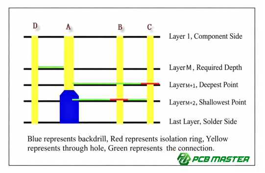
How Is Depth Accuracy Checked Using A/B/C/D Holes?
PCBMASTER uses multiple test points (A/B/C/D holes) to determine if the back drill is too shallow or too deep.
l Overly shallow drill: A/B/C holes remain connected, indicating residual stub is longer than desired.
l Overly deep drill: A/B/C holes are all open, potentially cutting functional copper. In this case, the connection between A and D holes is checked to ensure the via is still functional.
Production standard: Depth is considered acceptable if A and C holes are connected while B remains open, confirming the back drill reached the correct layer without compromising the signal path.
Example: On a 12-layer memory interface PCB, following this method ensured all back-drilled vias removed the stub while leaving active connections intact. This minimized reflections and transmission errors during high-speed testing.
What Is PCBM ASTER’s Testing Process and Quality Assurance?
PCBMASTER follows a step-by-step testing process to ensure high-speed signal integrity:
l Test pattern verification: Use designed A/B/C/D test points to validate theoretical back drill depth.
Electrical connectivity check: Confirm that functional layers remain connected, and stubs are removed.
l Signal integrity validation: Test high-frequency signals on sample boards to ensure reflections and transmission errors are minimized.
Case study: In a 16-layer PCIe PCB, PCBMASTER’s back drill testing confirmed correct depth for over 2000 vias. Signal testing showed improved 10 Gbps data transmission with significantly reduced reflections. This systematic approach ensures both reliable production and consistent high-speed performance.
What Is the Practical Value of Back Drilling in High-Speed PCBs?
Back drilling provides tangible performance improvements in high-speed PCB designs. It enhances signal quality, reduces transmission errors, and mitigates electromagnetic interference, offering both technical and economic benefits for complex multi-layer boards.
How Does Back Drilling Improve High-Speed Signal Transmission?
Back drilling removes unwanted via stubs, which are a major cause of signal reflection, distortion, and delay in high-speed circuits. By reducing stub length, signals maintain their integrity across multi-gigabit frequencies.
Example: On a 16-layer PCB carrying 10 Gbps PCIe signals, PCBMASTER back-drilled the stubs extending beyond active layers. Signal testing showed up to 20% less reflection and measurable reduction in transmission delay compared to non-back-drilled boards. This translates to fewer data errors, improved timing accuracy, and more reliable high-speed performance.
How Does Back Drilling Optimize EMC for High-Power Applications?
In high-power circuits, via stubs can act as tiny antennas, radiating unwanted electromagnetic noise. Back drilling eliminates these stubs, reducing EMI (electromagnetic interference) and improving electromagnetic compatibility (EMC).
Example: PCBMASTER applied back drilling to a multi-layer power amplifier board. Removing the stubs reduced noise coupling between high-speed traces and sensitive analog circuits. The result was a PCB that met EMC testing standards with minimal additional shielding or design changes.
What Are PCBMASTER’s Case Studies and Lessons Learned?
PCBMASTER has extensive experience applying back drilling to high-frequency, high-speed boards, balancing cost and performance.
Case study 1: A 12-layer memory interface PCB had long stubs causing reflections. Back drilling reduced residual stub depth to 5 mils, improving 8 Gbps signal transmission while maintaining manufacturing cost efficiency.
Case study 2: A 16-layer PCIe board required both high-speed signal integrity and low EMI. PCBMASTER optimized back drill depth and hole spacing, ensuring minimal reflections and meeting EMC standards without overcomplicating the design.
Lesson learned: Careful planning of back drill depth, layer selection, and stub tolerance allows high-performance results without significantly increasing cost. PCBMASTER emphasizes precision drilling, rigorous testing, and process optimization to achieve consistent outcomes.
What Are Common Back Drill Problems and How Are They Solved?
Back drilling can face issues such as depth errors, pad damage, and excessive stub residue. Addressing these problems is critical to maintaining high-speed signal integrity, PCB reliability, and manufacturing yield.
How Can Drill Depth Errors Cause Open or Short Circuits?
If the back drill is too deep, it can cut functional copper, creating an open circuit. If it’s too shallow, the stub remains, potentially causing signal reflections or even accidental shorts if the stub bridges nearby traces.
Example: In a 16-layer 10 Gbps PCB, PCBMASTER found that over-drilling one via completely cut the connection between layers 4–7. By implementing precise layer-specific depth calibration and machine tolerance checks, the team ensured back drills consistently removed the stub without damaging functional copper.
Solution: Always apply the “shallower is safer” principle, calibrate machines for board thickness, and use test patterns (like A/B/C/D holes) to verify drill depth before mass production.
How Does Pad Ring Damage or Insufficient Safety Spacing Affect PCBs?
Pad ring damage occurs when the back drill removes or cracks the via annular ring. Insufficient spacing between the back drill hole and nearby traces or pads can cause electrical shorts or weaken PCB reliability.
Example: On a 14-layer memory interface board, improper hole spacing caused minor pad ring fractures. PCBMASTER corrected this by increasing the drill-to-trace distance to at least 20 mils and maintaining 10–15 mil clearance from adjacent vias and outer pads.
Solution: Strictly follow IPC standards for minimum clearance, adjust drill size relative to original via, and inspect pads post-drilling to prevent damage. Proper spacing ensures safe, reliable multi-layer PCB operation.
How Does Excessive Stub Residue Cause Signal Loss?
If residual stubs are too long, they act as miniature antennas, causing signal reflections, scattering, and delay, which reduce high-speed signal quality.
Example: On a 16-layer high-speed PCIe board, PCBMASTER left 5 mil stubs after back drilling. Reducing them further to 4 mils minimized reflections and improved 10 Gbps signal transmission by 15–20%, without risking open circuits.
Solution: Control residual stub length through precise depth measurement, account for board thickness tolerances, and follow “as short as possible without cutting functional copper” rules. This ensures optimal signal integrity in high-speed PCB designs.
Conclusion
Back drilling is no longer an optional step in high-speed, high-frequency PCB design—it is essential for signal integrity, EMI control, and reliable multi-layer performance. By removing unwanted via stubs, carefully controlling drill depth, and following precise testing methods, engineers can dramatically reduce reflections, transmission errors, and electromagnetic interference.
PCBMASTER’s experience with complex, high-speed projects demonstrates that a well-planned back drill strategy balances performance, cost, and manufacturability. From layer-specific depth calibration to meticulous stub control and QA testing, every step ensures that high-speed digital and high-power boards achieve their full potential.
In today’s fast-paced electronics landscape, understanding and implementing proper back drilling is a key differentiator. With PCBMASTER’s proven expertise, your designs can meet the highest standards for signal quality, EMC compliance, and production reliability, giving your products a competitive edge.
FAQs
1. What is the difference between a back drill hole and a standard via?
A back drill hole is a modified via where the unnecessary copper stub beyond the functional connection layers is removed. Standard vias go through the entire board and may leave stubs that cause signal reflection. Back drilling improves high-speed signal integrity by eliminating these stubs without affecting the electrical connection of active layers.
2. What is the tolerance range for stub depth control?
Stub depth tolerance typically ranges from 4 to 8 mils depending on PCB thickness and machine precision. Controlling residual stub within this range ensures minimal signal reflection while avoiding damage to functional copper layers.
3. Does back drilling affect the structural strength of the PCB?
Back drilling slightly reduces the local mechanical strength around the via, but when properly controlled—considering hole diameter, safety spacing, and layer selection—it does not compromise the overall board integrity. PCBMASTER carefully plans drill size and spacing to maintain reliability.
4. What layer relationships need attention when back drilling multi-layer boards?
It is critical to specify the start and stop layers for each via. Only the copper beyond the functional layers should be removed. PCBMASTER ensures that back drills do not cut active layers and keeps proper spacing from adjacent vias, traces, and pads to prevent short circuits or open circuits.
5. How does PCBMASTER ensure signal integrity after back drilling?
PCBMASTER combines precise depth control, test patterns (A/B/C/D holes), and post-drill signal testing. Residual stubs are minimized, and high-speed signals are verified to reduce reflections and delay. This systematic process ensures that back-drilled PCBs meet the required signal quality standards for high-speed applications.

