







EV On-Board Charger PCB Design: Requirements, Challenges, and Best Practices
The PCB of an EV On-Board Charger (OBC) is the heart of an electric vehicle charging system. It allows the conversion of the AC power from the charging station to the DC power that the vehicle battery needs, while handling vital functions such as power regulation, protection and communication. The EV On-Board Charger PCB is the heart of the OBC system and directly influences the charging efficiency, safety, and long-term vehicle reliability.
The OBC PCB design is harder than a normal power supply PCB because it has to handle high voltage, high current, heat generation, electromagnetic interference and strict automotive reliability requirements at the same time. A small design mistake such as inadequate isolation distance or bad thermal management may impact the charging performance or even cause system failure during operation.
With years of experience in automotive PCB manufacturing, PCBMASTER understands that a reliable OBC PCB requires careful coordination between electrical design, material selection, PCB fabrication, and manufacturability. This article will cover the key design requirements, common engineering challenges, and practical best practices for designing high-performance EV On-Board Charger PCBs.
What Makes an EV On-Board Charger PCB Different?
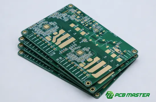
The EV On-Board Charger (OBC) PCB is unique from a regular power supply PCB as it needs to meet high voltage, high power, long-term reliability and stringent automotive safety standards simultaneously. A consumer power supply might operate a few hours a day but an EV OBC PCB should be able to provide stable performance for years under different temperature, vibration and demanding driving conditions.
High Voltage
An EV On-Board Charger PCB operates at much higher voltages than most electronic devices. Depending on the vehicle platform, it may handle hundreds of volts in battery charging. This requires sufficient creepage and clearance distances between conductive traces to avoid electrical arcing and insulation failure. A small spacing error can also increase the risk of electrical breakdown and reduce the reliability of the system.
High Power Density
Today’s electric vehicle needs to charge faster, but not make the charger bigger or heavier. Therefore, an OBC PCB should accommodate high-power components within a small space and should efficiently dissipate heat. For example, improper placement of components can lead to hot spots that reduce the lifetime of power semiconductors and capacitors.
Automotive Reliability
Consumer electronics do not need to operate reliably in the presence of vibration, humidity, dust and repeated temperature changes like an automotive OBC PCB must. Materials, solder joints, and PCB construction must be able to withstand years of continuous use without performance degradation, helping to ensure stable battery charging over the life of the vehicle.
Safety Requirements
Safety is one of the most important aspects in EV OBC PCB designing. The PCB must also isolate high and low voltage circuits, minimize electromagnetic interference (EMI) and support compliance with automotive safety and quality standards. A good PCB design can not only enhance the charging efficiency but also contribute to the protection of the vehicle, battery and its passengers in each charging cycle.
Key Design Requirements for an EV OBC PCB
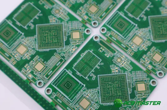
To have a successful EV On-Board Charger PCB design, you need to make some critical engineering decisions. The high voltage, high current, and high frequency switching technologies are integrated into an OBC system; thus, designers need to pay attention to electrical safety, heat generation, signal stability, and long-term reliability. PCBMASTER has extensive experience in manufacturing automotive PCBs and has seen firsthand how addressing these requirements early in the design process can reduce development risks and improve the performance of the final product.
High-Voltage Isolation
High voltage isolation is one of the most critical requirements in EV On-Board Charger PCB design. The purpose of it is to isolate high voltage power circuits from low voltage control circuits and keep the risk of electrical shock , short circuits and damage to components at minimum .
Proper creepage and clearance distances, insulated PCB materials and proper placement of components will give good isolation of OBC PCB. Creepage is the shortest path between two conductors by way of the surface of the PCB, clearance is the shortest distance through the air. Both must be compliant with automotive voltage and safety requirements.
For example, placing a high-voltage MOSFET near a control IC increases the likelihood of electrical arcing during voltage spikes. This is usually fixed by the designers by increasing spacing, adding isolation slots or using reinforced insulation as appropriate. These measures increase the electrical safety without greatly increasing the size of the PCB.
Good isolation also helps the charger to be more reliable over the lifetime of the charger especially when the charger is exposed to moisture, dust and temperature changes. Early consideration of isolation in the EV OBC PCB layout can reduce safety risks and contribute to compliance with automotive standards.
Thermal Management
Thermal management allows the EV On-Board Charger PCB to dissipate heat well and maintain stable performance. Heat is always produced by power conversion, so no cooling can reduce efficiency, decrease component life and increase the chance of failure.
The main sources of heat are power semiconductors, transformers, inductors and power resistors. During PCB design, engineers place these heat generating components to avoid hot spots. They also use thermal vias, large copper areas and thicker copper layers to draw heat away from critical devices.
For example, when a number of high power MOSFETs are packed closely together without sufficient heat dissipation, rapid charging can cause a rapid local increase in temperature. Thermal vias under the devices link to internal copper planes to help distribute heat more evenly across the board.
Thermal management should be designed in conjunction with the mechanical enclosure and cooling system. A properly designed EV OBC PCB helps to reduce the operating temperature, increase the charging efficiency and improve the reliability during the service life of the vehicle.
High-Current Routing
Proper routing of high currents is critical for an EV On-Board Charger PCB as it must be able to safely handle high charging currents with minimal power loss. Inefficient routing will lead to more electrical resistance, more heat generation and a potential decrease in overall charging efficiency.
Designers often employ wider copper traces, thicker copper foil and short, direct routing to support high current paths. The shorter the current path the less energy wasted and the smaller the voltage drop . This is different than power traces in many designs to reduce electrical interference.
A practical example of implementation is the relationship between the power converter and the battery output. If the copper traces are too narrow, they might heat up under continuous loading, which could lead to efficiency losses and long-term reliability issues. More copper = more current spread and lower operating temperatures .
The current flow should be balanced between the PCB as well. Careful routing enhances electrical performance and reduces the mechanical stress from uneven heating. Proper high current PCB layout increases efficiency, durability and stability in charging performance.
EMI/EMC Control
Electromagnetic noise is inherently produced by high-speed switching circuits, and EMI/EMC control is a key part of EV OBC PCB design. If left unchecked, this noise can interfere with nearby electronic systems, degrade charging performance, or cause the charger to fail compliance testing.
To reduce this electromagnetic interference ( EMI ), engineers attempt to keep the loops of high frequency current as small as possible, use continuous groundplanes, and to ensure that noisy power circuits are carefully separated from sensitive control signals . The use of input and output filters, shielding and proper groundings can improve the electromagnetic compatibility (EMC) .
For example, high speed switching traces routed directly below sensitive sensor circuits can couple unwanted noise into the control system. Moving these traces and making the PCB stack-up as optimal as possible can work wonders for the signal quality and system stability .
Good EMI/EMC PCB design is something you should consider as a starting point, not an end of line tweak. Early planning reduces redesign, shortens development time and makes sure the EV On-Board Charger PCB meets automotive EMC requirements.
Reliability for Automotive Applications
In automotive reliability, an EV On-Board Charger PCB needs to survive challenging environmental conditions for many years of safe operation. In contrast to consumer electronics, the electric vehicle charger experiences vibration, humidity, dust and repeated heating and cooling over its lifespan.
Improving reliability starts with selecting automotive grade PCB materials and components that will survive in the harsh operating environment. Good solder joints, balanced PCB stack-ups and adequate mechanical support can also help avoid failures due to thermal expansion or vehicle vibration.
For example, a heavy transformer that is poorly supported may cause continuous stress to the solder joints during driving. Stress relief and long-term durability are achieved by mechanical reinforcement or rearrangement of the components.
Manufacturing is also a key consideration. DFM (Design for Manufacturability) guidelines can be used to reduce the number of defects produced, and improve consistency over large production volumes. Engineers build an automotive OBC PCB that delivers stable performance, longer service life and reliable battery charging in real driving conditions, through the use of reliable materials, optimized layout and robust manufacturing processes.
Common Design Challenges
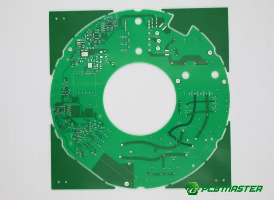
Designing a reliable EV On-Board Charger (OBC) PCB is a complex engineering task that requires addressing many intricate issues. The main challenge is to achieve a balance between the performance in power, thermal control, electrical safety and compact design in a limited PCB space. With PCBMASTER’s experience in automotive PCB manufacturing, many potential issues can be identified and improved at the design stage with proper engineering review and DFM analysis.
Heat dissipation
Thermal build-up is one of the biggest challenges in the design of EV OBC PCB. Charging causes significant heating of power devices like MOSFETS, SiC modules , transformers and inductors. If the heat is not sufficiently dissipated , the component temperatures increase and the efficiency is reduced and the service life shortened .
The usual fix is a combination of thermal vias , large copper planes , good spacing of components and good cooling methods like heatsinks or liquid cooling . This in turn prevents hot spots from developing on the PCB when heat sources are spread out rather than clustered together.
Switching noise
High-speed switching circuits improve charging efficiency, but they also generate electromagnetic interference (EMI). Excessive switching noise can interfere with control signals, communication circuits, and other nearby electronics, leading to instability or EMC test failures.
Engineers minimize switching noise by minimizing high-current loop areas, using continuous ground planes, isolating power traces and signal traces, and placing decoupling capacitors close to power devices. These types of layout methods improve signal integrity and reduce unwanted emissions.
Creepage distance
With the increase of charger power density, it is increasingly difficult to maintain sufficient creepage distance. While the desire to reduce the size of the PCB is common, reducing the spacing between high voltage conductors may increase the risk of electrical arcing, especially in humid or contaminated environments.
Engineers solve this problem by optimizing a PCB layout, increasing conductor spacing where needed, and by the use of isolation slots or insulating material in critical areas. These methods enhance electrical safety without compromising board size.
Component placement
Proper placement of components affects the electrical performance and the quality of manufacture. Power devices, magnetic parts and control circuits may cause overheating, longer current paths or more electrical noise without a well thought-out integration.
The practical answer is to group components by function, keep high current paths short and keep sensitive control circuits away from noisy power sections . This saves time and makes PCB assembly, test and maintenance easier.
Limited PCB space
Engineers designing modern electric vehicles have very little PCB real estate to work with when developing smaller, lighter and more powerful on-board chargers. The challenge is to add more functionality without compromising safety, cooling performance and reliability.
Optimized multilayer PCB stack-ups, careful routing, compact component selection and efficient layout planning all help successful designs make the most of the available space. Engineers will be able to optimize for higher power density while meeting performance and reliability requirements for automotive applications with early design consideration of space utilization.
Best Practices for OBC PCB Design
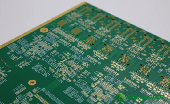
Designing a reliable EV On-Board Charger (OBC) PCB is not just a matter of electrical specification. In the development process, engineers need to consider power performance, safety, thermal efficiency, reliability and manufacturability. Proven design practices can reduce the failure probability, increase production efficiency and ensure stable operation in real world automotive environments. PCBMASTER’s experience in automotive PCB manufacturing demonstrates the value of early design optimization and tight integration between engineering and manufacturing teams in developing high-quality OBC PCB solutions.
Multi-layer PCB stack-up
A good multi-layer PCB stack-up is the foundation for reliable EV OBC PCB operation. An onboard charger is composed of high-power circuits, control signals and communication interfaces. A proper organisation of the various PCB layers is needed to improve the current distribution, to minimize electromagnetic interference and to ensure electrical isolation.
The power layers, ground layers and signal layers are normally separated by function. As an example, a power layer adjacent to a ground plane shortens the return-current path, thereby reducing noise and improving switching stability. And at the same time there are special isolation zones between high and low voltage circuits for extra safety.
According to the experience of automotive PCB projects from PCBMASTER, the stack-up shall be planned early in the design stage, instead of adjusting the stack-up after the layout is done. Engineers can consider layer structure, material selection, impedance requirements, and manufacturing capability in unison to achieve better electrical performance and avoid unnecessary redesign.
Thick copper where appropriate
The crucial factor in the design of high current EV OBC PCB is the selection of copper thickness. Onboard chargers can handle high charging currents but if the copper is not thick enough this can lead to high resistance, excess heat and reduced energy efficiency.
But copper-covering the whole PCB isn’t always the best answer. A better solution is to use thicker copper for high current areas such as power input paths, switching sections and battery output circuits and standard copper thickness for low current control areas.
For example, a high-current charging path should have a better continuous current-carrying capability than a communication circuit. By increasing the copper thickness in this area, the temperature rise is decreased and the long term reliability is improved.
PCBMASTER's manufacturing experience shows that the selection of copper thickness is a trade-off between the electrical requirements, the thermal performance, the PCB manufacturability and the cost. With good copper planning at design, customers can achieve reliable performance while reducing the complexity of production.
Proper grounding strategy
A robust grounding strategy is required for a stable operational environment of an EV On-Board Charger PCB. OBC systems have sensitive control electronics and high power switching circuits. Noise problems and system performance can be caused by poor grounding.
Engineers typically separate noisy power ground areas from sensitive signal ground areas and control where and how grounding connections are made. The return current paths are short and predictable, which damps voltage fluctuations and electromagnetic interference.
High frequency switching currents may share the same return path as sensor signals and therefore introduce noise into the control system. This may result in erroneous measurement or unstable operation. A good grounding design better controls the flow of current and avoids these problems.
During PCB design reviews such as return-current paths, layer arrangement and signal separation, e.g. the grounding performance is checked by PCBMASTER’s engineering team. Early optimization reduces EMI risks and increases the final automotive OBC PCB reliability.
Automotive-grade materials
The choice of materials has a direct impact on the reliability and lifespan of an EV On-Board Charger PCB. Consumer electronic products do not experience the same constant electrical stress, temperature variation, vibration and environmental exposure as automotive PCBs.
The best PCB materials should be stable in electrical performance, good thermal resistance and reliable mechanical strength. Dielectric properties, glass transition temperature (Tg) , thermal expansion and moisture resistance are factors that influence long term performance.
For example, an OBC under frequent fast charge conditions is subject to repeated heating and cooling cycles. The materials have better thermal stability, which leads to less stress on internal structures and improved durability.
Based on PCBMASTER’s experience on automotive electronics projects, the material selection needs to be adjusted to the specific requirements of the application, like voltage level, power output, operating temperature, and expected lifetime. The use of correct materials in the design of OBC PCB manufacturing process will result in a more reliable and consistent process.
DFM considerations
Design for Manufacturability (DFM) is an important practice to manufacture a reliable and cost effective EV OBC PCB. Manufacturing constraints, if not considered early in the design process, can result in manufacturing problems, even when the design is electrically correct.
DFM analysis considers the most important manufacturing considerations such as trace width, spacing, drill size, copper balance, via design, soldering and assembly. These checks will identify potential manufacturing risks before mass production.
For example, the via structure is too complex; or the spacing between features is too small, it may cause an increase in difficulty in fabrication and a decrease in production yield. It is usually easier and cheaper to make these changes while the design is being developed than after the prototypes have been built.
The DFM is an important part of the engineering process behind automotive PCB projects at PCBMASTER. Engineers work with customers to meet electrical requirements for manufacturability to help optimize designs before fabrication. This improves production consistency, reduces manufacturing risk and allows a smoother transition from prototype development to mass production.
Conclusion
A dependable EV On-Board Charger (OBC) PCB is essential for charging efficiency, electrical safety and long-term vehicle dependability. OBC systems are designed to operate in high voltage, high power and demanding automotive environments, therefore a successful OBC PCB design requires a balance between electrical performance, thermal management, EMI/EMC, and manufacturability.
Based on the experience of PCBMASTER in automotive PCB manufacturing, early collaboration of design and manufacturing team can help to find out the potential risks before production. During the development stage, engineers can optimize PCB structure, select proper materials and improve DFM considerations to shorten development cycles, improve production consistency and build more reliable EV On-Board Charger PCB solutions for modern electric vehicles.
Frequently Asked Questions About EV On-Board Charger PCB
1. What is an EV On-Board Charger PCB?
The PCB of the EV On-Board Charger is the main circuit board of the on-board charger system of electric vehicles . It regulates the changeover of the alternating current (AC) from the charging source to the direct current (DC) power to the vehicle’s battery. The PCB performs important functions such as power conversion, voltage regulation, protection and communication between charging components.
2. Why is OBC PCB design more challenging than standard power supply PCB design?
PCB design for OBC is more challenging because of high voltage, high current, high power density and harsh automotive environment at the same time. In addition to the usual power supply PCBs, an automotive OBC PCB must meet stringent requirements for electrical isolation, thermal management, EMI/EMC control, and long-term reliability.
3. What are the most important design considerations for an EV OBC PCB?
The key design challenges for an EV On-Board Charger PCB include high voltage isolation, thermal management, high current routing, EMI/EMC control and automotive reliability. The PCB stack-up, copper thickness, grounding strategy, material choice, and component placement all need to be carefully optimized by engineers for safe and efficient operation.
4. How can engineers improve the reliability of an OBC PCB?
Engineers can enhance the reliability of OBC PCBs by using automotive-grade materials, optimizing thermal paths, ensuring proper creepage and clearance distances, managing electromagnetic interference, and applying Design for Manufacturability (DFM) principles. Getting manufacturing involved early in the process and in design reviews can help identify potential problems before they become issues in mass production.
5. Why is choosing an experienced automotive PCB manufacturer important for OBC PCB projects?
An experienced automotive PCB manufacturer can greatly assist with material selection, stack-up optimization, DFM analysis and production quality control. For complex applications such as EV On-Board Charger PCBs, working with a manufacturer such as PCBMASTER can help to reduce development risks, improve manufacturing consistency and speed up the transition from prototype to mass production.
About the Author

Carol Luo
PCB Design EngineerI'm Carol, a PCB Engineer at PCBMASTER with experience in PCB design and manufacturing engineering since 2018. I focus on translating engineering requirements into reliable PCB solutions, with expertise in stack-up design, material selection, and design-for-manufacturing (DFM). I share practical engineering insights from real-world PCB design and production experience.
Visit Carol Luo's Profile