








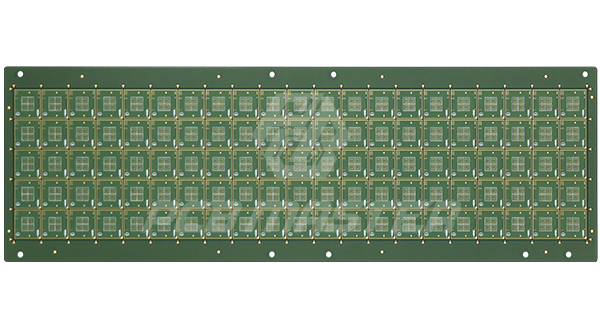
2-layer IC packaging substrate
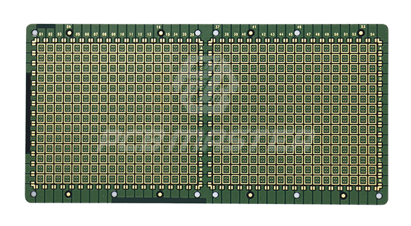
Product Specifications
- Material BT
- Layer 2-layer
- Thickness 0.3mm
- Surface finish Electroless Nickel - Palladium - Gold: Nickel thickness 120 - 240U, Palladium thickness: 2U, Gold thickness: 2U
- Min Track/Spacing 0.05/0.05mm
- Special process The Subtractive process flow is adopted.
- Min hole size 0.1mm
- Special technology Small hole diameter, small trace width and trace spacing. The concentricity requirement for the circuits on both sides of the product is 0.05mm.
Related Products
Ready to start your project?
Get a quote today or contact our technical team for assistance.

