








What Is Delta-L Testing? A Complete Guide to PCB Insertion Loss Measurement
Modern high-speed electronics are pushing PCBs to their performance limits. As data rates increase in AI servers, data centers, networking equipment, and advanced computing systems, even small amounts of signal loss can impact reliability and overall system performance. Accurate insertion loss measurement is therefore an important part of PCB design, material selection, and manufacturing validation.
Delta-L testing has become one of the most trusted methods for measuring transmission line loss because it isolates the performance of the PCB trace itself while minimizing measurement errors from probes, fixtures and vias. But what exactly is Delta-L testing, how does it work and why has it become an industry standard for high-speed PCB verification? In this guide, we'll explain the working principle, key advantages, coupon design requirements, differences between Delta-L 3.0 and 4.0 and the critical factors that affect measurement accuracy.
What Is Delta-L Testing?
The Delta-L test is a high speed PCB measurement technique. The Delta-L test is the measurement of the insertion loss of a transmission line by measuring two test traces of different length . It helps engineers to better understand the electrical performance of PCB materials and manufacturing processes .
As the signal speed continues to increase, the measurement of insertion loss has become an important part to guarantee reliable signal transmission. Delta-L testing differs from the traditional measurement methods in that it removes most errors introduced by probes, connectors, fixtures and vias, and the results can represent the PCB transmission line itself. It is now widely used in AI servers, data centers, network equipment, and other high-speed electronic applications.
Definition of Delta-L testing
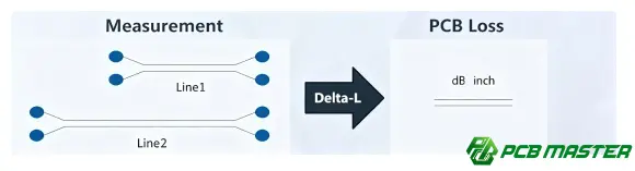
Delta-L testing is a differential insertion loss measurement technique that measures signal loss per unit length by comparing two nearly identical PCB transmission lines of different length.
The name Delta-L comes from “ Delta Length (ΔL) ”, which is the difference in length of two test traces. Both traces are designed to have the same stack-up, impedance, trace width, trace spacing, vias, probe pads and reference planes. The only intentional difference is the trace length.
The testing process is straightforward:
- Measure the insertion loss of the short trace.
- Measure the insertion loss of the long trace.
- Subtract the two results.
- Divide this difference by the difference in trace length (ΔL).
The final result is the loss per unit length in dB/in or dB/cm. This value is easy to use to compare different PCB materials, manufacturing processes or board designs when tested under the same conditions.
For example, if two coupons differ in trace length by 10 cm and in measured insertion loss by 2 dB, the computed insertion loss is 0.2 dB/cm. This information can be used by engineers to compare the performance of different PCB laminates or to verify if a finished PCB meets high-speed design requirements.
Why Intel developed the Delta-L method
Intel developed the Delta-L method to measure PCB insertion loss more accurately by eliminating errors caused by the testing setup instead of the PCB transmission line itself.
In high-speed PCB testing, a direct insertion loss measurement includes not only the loss of the PCB trace but also the loss from probes, connectors, test fixtures, and vias. As operating frequencies increase, these extra losses become more significant and make it difficult to determine the true performance of the PCB.
Delta-L solves this problem by comparing two transmission lines that are identical except for their length. Because both traces use the same measurement setup, most common errors appear in both measurements and cancel out when the results are subtracted. The remaining difference represents only the loss introduced by the additional trace length.
A simple comparison helps explain the idea. Imagine you weigh two identical boxes . One just happens to have an extra book in it . Since the boxes themselves weigh the same, the weight difference tells you the weight of the book alone. Delta-L uses the same principle to isolate the insertion loss of the PCB transmission line.
This results in more repeatable and reliable results, making Delta-L testing an industry standard method to qualify PCB materials, validate manufacturing quality, and support high-speed interfaces such as PCIe, Ethernet, USB and DDR.
Why Is Delta-L Testing Important for High-Speed PCB Design?
Delta-L testing is critical because today’s high speed electronic systems are more sensitive to signal loss than older designs. It provides an accurate measure of the insertion loss of a PCB, enabling engineers to select the appropriate materials, optimize PCB manufacturing, and ensure reliable transmission of signals. As data rates continue to climb, even small losses can negatively affect system performance. Delta-L testing enables engineers to measure the electrical performance of PCB transmission lines with minimal measurement errors from the test setup. As such, it is one of the most reliable ways to validate high-speed PCB designs.
Increasing signal loss at higher data rates
At higher data rates the signals contain higher frequency components which attenuate more as they travel down PCB transmission lines.The faster the signals, the more power it will lose while traveling through copper traces and PCB dielectric materials. This is called insertion loss, and it gets worse as frequency increases. A PCB that works well at a low data rate may not cut it for the next-generation communication standards.Several factors contribute to higher signal loss such as:
- Dielectric loss of PCB material
- Loss of copper conductor
- Surface roughness of copper
- Discontinuities of via
- Longer transmission lengths
For example, a PCB designed for PCIe Gen3 can work reliably but the same board can experience excessive signal attenuation when upgraded to PCIe Gen6. Accurate measurement of insertion loss helps engineers to find out whether the PCB can support these higher speed applications before products go into mass production.
How insertion loss affects signal integrity (SI)
Higher insertion loss attenuates electrical signals and makes it more difficult for the receiver to accurately determine what data was transmitted. Signal Integrity (SI) refers to the signal’s ability to preserve its original shape as it travels through a PCB. Excessive insertion loss can reduce the signal amplitude, distort the waveform and increase the possibility of communication errors.The typical symptoms of excess insertion loss are:
- Reduced eye openings in eye diagrams
- Increased bit error rate (BER)
- Decreased communication distance
- Reduced system reliability
- Greater likelihood of data transmission failures
Imagine a person speaking across a large room. The farther they are away, the weaker and more difficult to understand their voice is. Likewise, electrical signals attenuate as they travel through a lossy PCB channel. Delta-L testing allows engineers to measure this loss so they can improve PCB materials or optimize the board design before problems develop.
Why modern interfaces require accurate loss measurement
Modern high speed interfaces operate at very high frequencies where there is little margin for signal loss. Accurate insertion loss measurement is critical to guarantee stable communication.Many of today's communication standards specify tight channel loss requirements. If the PCB exceeds these limits, the system may fail compliance testing or operate unstably.Like:
- PCIe: The data rates for graphics cards, SSDs, and AI accelerators are ever increasing and each new PCIe generation is ramping up bandwidth and with this insertion loss becomes a critical design parameter.
- Ethernet: To get reliable network performance, low-loss PCB channels are needed for high-speed Ethernet standards such as 100G, 400G and 800G.
- USB: USB4 and other high speed USB standards use controlled impedance and low insertion loss to ensure stable data transfer.
- DDR: High-speed memory interfaces need a consistent quality of signal to keep the processor and memory devices in sync.
- AI servers: AI computing platforms have many high-speed interconnects between CPUs, GPUs, memory modules and network devices. Low-loss PCB transmission lines help to maintain system performance under heavy workloads.
- Data centers:Today’s data centers process huge quantities of information every second. Precise PCB insertion loss measurement helps to guarantee dependable communication between servers, switches and storage systems, while reducing signal-related failures.
These applications operate with very small signal margins, so even small increases in insertion loss can impact the overall system performance. Delta-L testing provides engineers with reliable data to validate their PCB designs before deployment.
Why Delta-L has become an industry-standard validation method
Delta-L has become an industry-standard validation method because it measures PCB insertion loss accurately and minimizes errors caused by probes, fixtures, connectors and vias.Unlike direct insertion loss measurements, Delta-L compares two nearly identical transmission lines with different lengths. Since both measurements include the same test equipment and structures, most common measurement errors cancel out during the calculation. The remaining result closely represents the loss of the PCB transmission line itself.There are several important benefits to this approach:
- High measurement accuracy
- Good repeatability of tests
- Reasonable comparison of different PCB materials
- Reliable assessment of manufacturing consistency
- Suitability for modern high-speed PCB standards
For example, a PCB manufacturer designing a new low-loss laminate could use Delta-L testing to compare several material options under the same conditions. As the measurement errors from external sources are largely eliminated, engineers can be confident that any variations in insertion loss are attributed to the material itself and not the measurement setup.
As high-speed technologies continue to evolve, Delta-L testing has become a trusted means of verification throughout the PCB industry, enabling manufactures, material suppliers and OEMs to qualify products for advanced applications like PCIe Gen5, PCIe Gen6, 800G networking, AI servers and next-generation data center infrastructure.
How Does Delta-L Testing Work?
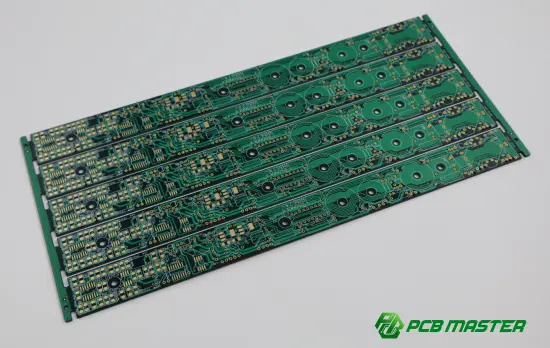
Delta-L testing measures two almost identical PCB transmission lines of different lengths and compares their insertion loss . This way, the losses both measurements share are eliminated and the method provides an accurate calculation of the insertion loss per unit length of the PCB trace.
Delta-L does not measure a single transmission line, but instead measures the difference between a short coupon and a long coupon. This allows the engineer to look at the performance of the PCB transmission line itself, minimizing the effects of the probes, connectors, fixtures and vias.
Basic principle of differential measurement
Delta-L testing uses differential measurement to eliminate common measurement errors and isolate the loss due only to the additional trace length.
The basic idea behind Delta-L testing is that the two test coupons are nearly identical. They use the same PCB material, layer stack-up, differential impedance, trace geometry, probe pads, vias, and reference planes. The only intentional difference is the transmission line length.
Because both coupons are measured with the same equipment and setup, most external losses remain the same in both tests. When the insertion loss of the short coupon is subtracted from the insertion loss of the long coupon, these common losses largely cancel out.
Think of it like weighing two identical bottles except one has a little more water in it. The bottles weigh the same so the difference in weight is just the extra water. Delta-L does the same thing to isolate the insertion loss due to the extra PCB trace length.
Comparing two transmission lines with different lengths
Delta-L compares a short transmission line and a long transmission line that are identical in every way except for length.
The two test structures are named Delta-L coupons. They are designed with one important rule: all electrical and physical characteristics are the same except for the length of the trace.
To obtain accurate results, both coupons must be identical in the following characteristics:
- PCB material
- Layer stack-up
- Controlled impedance
- Trace width and spacing
- Copper thickness
- Probe pad design
- Via count and structure
- Ground reference planes
Any variation in these parameters will cause the measured loss to be influenced by other variables and will not accurately reflect the effect of the extra trace length alone. This is why careful coupon design is so critical for reliable Delta-L testing.
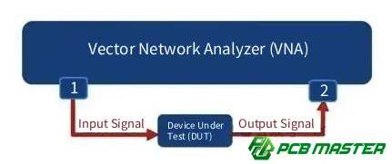
Measuring S-parameters using a Vector Network Analyzer (VNA)
A Vector Network Analyzer (VNA) measures the S-parameters for each coupon that engineers can use to calculate insertion loss over a wide band of frequencies.
The primary instrument for Delta-L testing is a Vector Network Analyzer which injects high frequency signals into the PCB transmission line and measures the amount that gets through and the amount that is reflected back .
The most important parameter for Delta-L testing is S21, also called insertion loss. By measuring the S21 response of the short and long coupons, the engineer can determine how much additional loss is caused by the extra length of transmission line.
Today's VNAs measure frequency from several GHz to more than 40 GHz, making them ideal for verifying high-speed PCB designs for PCIe Gen5, PCIe Gen6, 800G networking and other emerging applications.
How insertion loss per unit length is calculated
Delta-L calculates insertion loss per unit length by subtracting the insertion loss of two coupons and then dividing by the difference in their length (ΔL).
There are four simple steps to the calculation.
Measure the short coupon
Measure insertion loss of the short coupon with the VNA. This result includes losses from the PCB trace, probe pads, vias, connectors, and test fixtures.
Measure the long coupon
Measure the long coupon using the same VNA, calibration method, probes and test conditions. Since the coupons have the same structure, most of the external losses are almost identical.
Calculate the insertion loss difference
Subtract the insertion loss of the short coupon from the insertion loss of the long coupon.
This difference is the extra loss of signal caused by the extra length of transmission line . Most typical measurement errors are eliminated .
For example:
- Short coupon insertion loss: 3 dB
- Long coupon insertion loss: 5 dB
- Additional insertion loss: 2 dB
Divide by the length difference (ΔL)
Finally, divide the additional insertion loss by the difference in length between the two coupons.
- Length Difference: 10 cm
- Added insertion loss: 2 dB
Insertion Loss per Unit Length = 2 dB ÷ 10 cm = 0.2 dB/cm
This normalized value allows engineers to compare different PCB materials, manufacturing processes or board designs irrespective of the total trace length.
Why this method improves measurement accuracy
Delta-L improves measurement accuracy by eliminating most of the losses caused by the test setup and leaving only the loss of the PCB transmission line.
Many unwanted factors such as probe transitions, connectors, fixtures and via discontinuities are included in direct insertion loss measurements, which can make it difficult to determine whether the measured loss is from the PCB itself or the measurement system.
Delta-L reduces this uncertainty by comparing two nearly identical coupons under the same test conditions. Since both measurements include the same external losses, those losses are largely canceled during the calculation.
The result offers several important benefits:
- More accurate insertion loss measurement
- Better repeatability between different tests
- More reliable comparison of PCB materials
- Easier identification of manufacturing variations
- Higher confidence in high-speed PCB validation
For example, if two PCB laminates appear to have different insertion loss values in a direct measurement, it may be unclear whether the difference comes from the material or the test setup. Delta-L removes most common measurement errors, making it much easier to identify the true electrical performance of each material. This is one of the main reasons why Delta-L testing has become a widely accepted method for qualifying high-speed PCBs.
Why Doesn't Delta-L Measure a Single Trace Directly?
Delta-L cannot measure a single PCB trace directly because the insertion loss you measure will include losses from the whole test setup, not only from the transmission line itself. By comparing two traces with different lengths, Delta-L removes most shared measurement errors and provides a more accurate result.In high-speed PCB testing, the signal travels through much more than the PCB trace. It also passes through probes, connectors, fixtures, and vias before reaching the measurement instrument. These components all introduce additional insertion loss and reflections. If engineers measured only one trace, it would be difficult to determine how much of the loss came from the PCB itself.
Sources of measurement error
Direct insertion loss measurements include several unavoidable sources of error that can affect the accuracy of the test results.
The following components can all contribute additional loss or impedance discontinuities during measurement.
Probe Loss
High-frequency probes connect the Vector Network Analyzer (VNA) to the PCB test coupon. Although they are carefully designed for microwave measurements, probes still introduce a small amount of insertion loss and impedance mismatch, especially at very high frequencies.
As testing frequencies increase, probe performance becomes more critical. Even small probe-related losses can influence the measured results if they are not removed from the calculation.
Connector Loss
Some test setups use RF connectors or adapter cables between the VNA and the PCB. These connectors are not 100 % lossless and may introduce additional attenuation or reflections.
Connector quality, manufacturing tolerances and re-use can also cause small variations between measurements, reducing the repeatability of testing high-speed PCB transmission lines.
Loss Fixture
Loss A test fixture is used to hold the PCB coupon in place and to provide the electrical connection to the measurement equipment. Like any transmission path, the fixture has its own insertion loss and impedance characteristics.
If fixture loss is included in the measurement, engineers cannot easily determine whether the measured attenuation comes from the PCB trace or from the fixture itself. This becomes more noticeable when testing low-loss PCB materials.
Via Discontinuities
Many PCB test coupons use vias to connect signal traces between different layers. Some designs require vias which create impedance discontinuities that can cause signal reflection and additional insertion loss.
Long stubs are especially problematic because they can be resonant at high frequencies and so increase signal degradation. Modern high-speed PCB designs often use back drilling or Via-in-Pad Plated Over (VIPPO) to reduce these unwanted effects.
How Delta-L removes common-mode measurement errors
Delta-L removes common-mode measurement errors by comparing two nearly identical test coupons measured under the same conditions.
Both the short coupon and the long coupon use the same PCB material, stack-up, probe pads, vias, fixtures, probes, connectors, and measurement equipment. The only intentional difference is the trace length.
Because the measurement setup is identical, most external losses appear in both results. When the insertion loss of the short coupon is subtracted from that of the long coupon, these shared losses largely cancel out. The leftover difference is the loss that the additional length of transmission line introduces.
This is called differential measurement, where the importance is on the difference between two measurements, not on the absolute value of one measurement.
The simple example is to measure two identical ropes, one 10 meters longer than the other, and then the difference in weight is almost all due to the extra length and not the scale or environment. Delta-L applies the same idea to better measure insertion loss.
Advantages over direct insertion loss measurement
Delta-L offers greater accuracy, repeatability and a more reliable assessment of PCB transmission line performance than direct measurement.
Delta-L measures the insertion loss of the PCB trace itself, rather than all losses together. This makes the results much more useful for comparing PCB materials or validating manufacturing quality.
Key advantages are:
- Higher accuracy: most losses caused by probes, connectors, fixtures and other shared measurement components have been eliminated.
- Better repeatability: More consistent results when measurements are repeated under the same conditions.
- Fair material comparison: It reduces external measurement error, and so makes it easier to compare different PCB laminates.
- Improved process evaluation: Assists in determining if the changes in insertion loss are due to differences in PCB materials or manufacturing.
- Industry acceptance: High-speed PCB qualification and insertion loss validation for PCB manufacturers, material suppliers and OEMs.
For example, two PCB materials may have slightly different values for insertion loss when measured directly. Without Delta-L, it can be difficult to know whether the difference is due to the materials or the test setup. By removing most common measurement errors, Delta-L makes a simpler comparison and allows engineers to make more confident design and manufacturing decisions.
What Equipment Is Required for Delta-L Testing?
Delta-L testing is an expensive process requiring specialized equipment to accurately measure PCB insertion loss at high frequencies. The key tools are a Vector Network Analyzer (VNA), high frequency probes, a properly designed Delta-L test coupon, calibration standards and supporting fixtures and analysis software.
Each piece of equipment has a different role in the measurement process. High quality equipment and correct test procedure helps to ensure that the measured insertion loss is a reflection of the PCB transmission line performance and not errors from the measurement system.
Vector Network Analyzer (VNA)
The Vector Network Analyzer (VNA) is the main instrument used in the Delta-L testing to measure the S-parameters of a PCB transmission line .
The VNA creates high frequency signals and sends them through the PCB test coupon to see the signals behavior as they travel down the transmission line. From those observations the engineers can figure out key electrical parameters like insertion loss and return loss.
For Delta-L testing, the most important parameter is S21. S21 is the insertion loss of the transmission path.
The VNA for high-speed PCB testing should provide: Wide frequency coverage High measurement accuracy Stable and repeatable results Support for differential signal measurements For example, Delta-L 3.0 testing requires measurements up to about 20 GHz, while Delta-L 4.0 can require measurements up to 40 GHz or more to support advanced interfaces such as PCIe Gen6 and 800G Ethernet.
High-frequency probes
The high frequency probes offer a well controlled impedance connection from the VNA to the Delta-L coupon with minimal signal distortion.
High frequency probes are not your standard electrical probes, they are designed specifically for microwave and high speed signal measurements. They directly contact the probe pads on the PCB coupon providing a stable signal path between the VNA and the transmission line.
A good probe should be able to give you :
- Low insertion loss
- Stable electrical contact
- Controlled impedance
- High bandwidth frequency
- Good measurement repeatability
The importance of probe selection increases with increasing testing frequencies . Even small impedance mismatches between the probe and the PCB can create reflections that can affect the measurement accuracy . This is one of the reasons why modern Delta-L coupon designs pay special attention to the probe pad geometry and launch transitions.
Delta-L test coupon
A Delta-L test coupon is a specially designed sample of a PCB that is used to measure insertion loss by comparing two transmission lines of different length.
The coupon is one of the most important components of the whole measurement procedure. It consists of a short and a long transmission line which are identical except for their length.
For consistent results, the two coupons should match in the following:
- PCB material
- Layer stack-up
- Differential impedance
- Trace width and spacing
- Via structure
- Probe pad design
- Ground reference
The only difference should be the length of the transmission line. This allows Delta-L testing to isolate the insertion loss due to the extra length of trace, minimizing the effect of other variables.
If the long coupon had different vias or a different pad design, the measured difference will not be a simple transmission line loss.
Calibration methods
Calibration removes measurement equipment errors before the Delta-L testing begins, improving accuracy of the final results.
The VNA is calibrated with known reference standards before measuring the Delta-L coupon. The calibration provides measurement reference plane and corrects for the losses from the cables, connectors and probes.
Common calibration methods include:
- SOLT (Short, Open, Load, Through)
- TRL (Thru, Reflect, Line)
- Probe-tip calibration for on-wafer or pcb probing
The calibration method used depends on the test setup and frequency range. For many high speed PCB measurements, TRL calibration is often the method of choice, as it provides excellent accuracy for transmission line measurements at microwave frequencies.
Inaccurate calibration of equipment can introduce measurement errors that reduce repeatability and make it difficult to compare results between different PCB materials or manufacturing lots.
Test fixtures and software
Test fixtures hold the PCB coupon in place during measurement.The analysis software takes the measured data and calculates Delta-L results.
The test fixture provides mechanical stability and repeatable electrical connections between the test equipment and the PCB coupon. A good fixture will limit unwanted movement and help to keep reliable probe contact during the test.
The S-parameter data is then post-processed with specialized software to calculate insertion loss per unit length. The software can also be used to generate frequency response curves, compare multiple test results and identify trends between different PCB materials or manufacturing processes.
Typical software features include: Import S-parameter files Calculate insertion loss per unit length Compare long and short coupon measurements Frequency response graphs Export engineering analysis report For example, a PCB manufacturer who wants to evaluate several low loss laminates may use the software to compare the Delta-L results across all samples, thus making it easier to determine which material provides the best high frequency performance. Fixture and software work together to help ensure that Delta-L testing produces accurate, repeatable and easy-to-analyze results.
What Is a Delta-L Test Coupon?
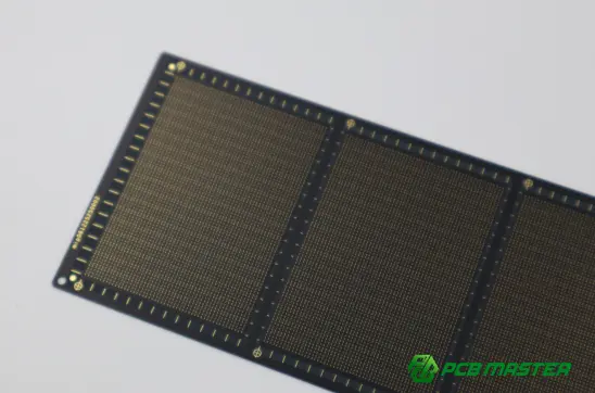
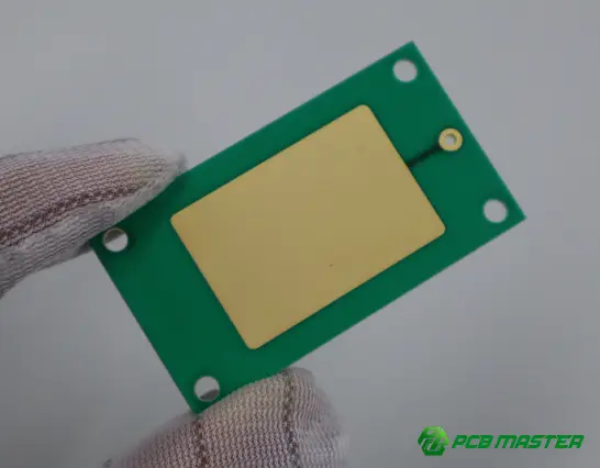
A Delta-L test coupon is a special structure on a PCB that is used to measure insertion loss accurately. It consists of two almost identical transmission lines, one short and one long, that are identical except for length. This allows an engineer to determine the insertion loss per unit length and minimize errors in the measurements.
The Delta-L coupon is built specifically for electrical testing, not a functioning PCB. The coupon is designed under strict design rules so the measured results reflect the performance of the PCB transmission line, not the effect of probes, vias or other structures. The Delta-L test coupon has become an essential tool for validating high-speed PCB materials and manufacturing quality, due to its accuracy and repeatability.
Purpose of a Delta-L coupon
A delta-L coupon is used to give an accurate measurement of the insertion loss of a transmission line on a PCB.
The Delta-L coupon lets the engineer compare two transmission lines that are identical in every way except length. By measuring both coupons under identical conditions, common losses in the measurement setup cancel out, leaving only the loss from the extra length of trace.
Typical uses of the Delta-L coupon are:
- Insertion loss/length measurement
- Comparison of different PCB materials
- Verification of PCB manufacturing quality
- Validation of impedance controlled PCB designs
- Support for high-speed interface qualification
For example, a PCB manufacturer could build the same coupons with two different low-loss laminates. The comparison of the Delta-L test results would allow engineers to identify the material with lower insertion loss for PCIe Gen6, 800G Ethernet or AI server applications.
Long coupon vs. short coupon
The short coupon and long coupon are similar in structure and design. The only intentional difference is the length of the transmission line.
The insertion loss per unit length is calculated by dividing the difference of the insertion loss between two coupons by the difference of the length (ΔL) using same test equipment.
| Feature | Short Coupon | Long Coupon |
|---|---|---|
| Primary purpose | Reference measurement | Measure additional transmission line loss |
| Transmission line length | Shorter | Longer |
| PCB material | Same | Same |
| Layer stack-up | Same | Same |
| Controlled impedance | Same | Same |
| Trace width and spacing | Same | Same |
| Probe pads | Same | Same |
| Via structure | Same | Same |
| Ground reference | Same | Same |
| Measurement equipment | Same VNA and probes | Same VNA and probes |
| Expected insertion loss | Lower | Higher |
Since all design features are the same except for the trace length, the measured difference accurately characterizes the loss introduced by the extra transmission line.
Why only the transmission line length should differ
Only the transmission line length should be different because Delta-L testing assumes everything else is the same. Then, the measured difference is due to the insertion loss introduced by the added trace length.
If the two coupons differ in other features, additional loss or reflections can be added and make the calculation inaccurate.
These include:
- PCB laminate material
- Layer stack-up
- Differential impedance
- Trace width and spacing
- Copper thickness
- Copper surface roughness
- Probe pad geometry
- Via design and quantity
- Ground reference planes
- Manufacturing process
For example, the long coupon has a larger probe pad than the short coupon, and therefore some of the measured loss could be due to the pad transition and not the additional transmission line. Also, an additional via added to one coupon creates additional discontinuities that affect insertion loss. If all the design parameters are the same, Delta-L testing can isolate the true electrical performance of the PCB trace.
Typical coupon structure
A typical Delta-L coupon is constructed of carefully designed transmission lines, probe interfaces and reference structures that allow for precise high frequency measurements.
Exact layout may vary depending on the Delta-L specification (or PCB manufacturer) but most coupons contain the same basic elements.
A typical Delta-L coupon consists of:
- Probe pads: Used for electrically connecting the high frequency probes to the PCB.
- Launch transition :Smooth transition from the probe pads to the transmission line to minimize impedance discontinuities .
- Differential transmission line: The primary test trace for insertion loss measurement
- Via structures Connect signal traces between PCB layers: They maintain electrical properties .
- Continuous Ground Planes: Provide a stable return path and help with impedance control .
- Reference markers:Support with alignment, measuring and quality check during testing.
A Delta-L coupon is a standardized test track for electrical signals. A race track is designed to measure the performance of a vehicle under controlled conditions. Likewise a Delta-L coupon is designed to measure the performance of a PCB transmission line minimizing the effects of external influences. This standard structure allows engineers the ability to compare PCB materials, manufacturing processes and high-speed designs with confidence and repeatability.
How Should a Delta-L Coupon Be Designed?
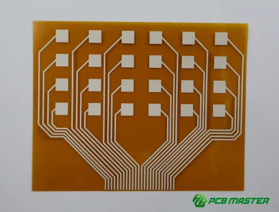
A Delta-L coupon should be designed so that the measured insertion loss reflects the performance of the PCB transmission line—not the effects of pads, vias, probes, or layout differences. The coupon has to be controlled impedance, have the same structures, have smooth signal transitions and have consistent routing all along the test path.
A well designed Delta-L coupon improves the measurement accuracy and repeatability. Even minor design changes can create impedance discontinuities, reflections or additional insertion loss making it difficult to assess the true electrical performance of the PCB.
Maintain controlled impedance throughout the trace
The target impedance should be controlled along the entire transmission line from one end of the coupon to the other in order to avoid unwelcome reflections and wrong insertion loss measurements.
One of the most important requirements for a Delta-L coupon is controlled impedance. If the impedance changes anywhere along the transmission line, some of the signal will be reflected rather than making it to the receiver. These reflections affect both insertion loss and return loss.
There are various design factors that help keep the impedance the same .
Trace width
he width of the trace directly affects the characteristic impedance of the transmission line. Even small manufacturing variations can change the impedance and affect the high frequency performance.
The trace width should:
- Match the target impedance (e.g. 85 Ω or 100 Ω differential)
- Be consistent across the coupon
- Meet the PCB manufacturer’s impedance calculations
Trace spacing
The spacing of the differential pair is just as important as the trace width.
Consistent spacing helps to:
- Maintain differential impedance
- Reduce signal skew
- Improve signal integrity
- Produce more repeatable Delta-L results
Do not vary the spacing along the routing path unless the design rules require it.
Dielectric thickness
The distance between the signal layer and the reference plane has an impact on impedance and insertion loss.
A stable dielectric thickness provides:
- Repeatable impedance
- Predictable signal velocity
- Improved repeatability of measurements
PCB materials with controlled dielectric thickness reduce variation from production batch to production batch.
Copper thickness
Copper thickness affects the electrical properties of the transmission line. If the copper thickness is significantly different the impedance may also be different.
To achieve accurate Delta-L testing:
- The coupons must have the same thickness of copper.
- Control plating thickness during Manufacturing.
- Avoid thickness variations in production lots.
Keep long and short coupons identical except for length
The long and short coupons should be identical in all design details except for the length of the transmission line.
This is the basic premise of Delta-L testing . The technique assumes the only thing effecting insertion loss is the extra length of the trace .
The following features should be kept constant:
- PCB material
- Layer stack-up
- Controlled impedance
- Trace width and spacing
- Probe pads
- Via design
- Ground planes
- Copper roughness
- Manufacturing process
For example, if one coupon contains an additional via or a different pad shape, the measured insertion loss difference will be affected by these additional effects and the accuracy of the Delta-L calculation will be reduced.
Optimize probe launch design
The probe launch should have a smooth electrical transition from the probe pads to the transmission line with minimal impedance variations.
The launch area is one of the most sensitive parts of a Delta-L coupon because it is where the measurement equipment connects to the PCB.
A poor launch design can introduce reflections before the signal even reaches the transmission line.
Pad size
Probe pads should be large enough for reliable contact but no larger than necessary.
Oversized pads can:
- Change the local impedance
- Increase signal reflections
- Reduce measurement accuracy
Modern Delta-L 4.0 coupons typically use smaller pad designs than earlier versions to reduce these effects.
Smooth trace transition
The signal path should smoothly transition from the probe pad into the transmission line.
Smooth transition helps in minimization of impedance changes, return loss and improves the signal transmission. Sharp corners or abrupt change in trace width should be avoided as much as possible.
Minimize impedance discontinuity
Any discontinuity in the path of the signal can cause an impedance discontinuity.
The common causes are: Large probe pads Sudden trace widening Abrupt routing changes Poor launch geometry Making the signal path smooth and continuous, the measured insertion loss is more likely to be a representation of the transmission line, as opposed to the launch structure.
Minimize via stub effects
Keep via stubs as short as possible . They can create signal reflections and resonance at high frequencies .
The unused portion of a via which extends beyond the signal layer is called a via stub. At high frequencies, this unused section behaves like a small resonator, increasing insertion loss and degrading signal integrity.
Two common techniques help reduce these effects.
Back drilling
Back drilling removes the unused section of a plated through-hole after PCB fabrication.
It benefits are:
- Shorter via stubs
- Less signal reflections
- Better high frequency performance
- Better insertion loss results
Back drilling is a common technique used in high speed PCBs for applications such as AI servers and high speed networking equipment.
Via-in-Pad Plated Over (VIPPO)
VIPPO places the via directly in the component pad and fills and plates over to form a flat surface.
Compared with traditional via designs,VIPPO provides:
- Shorter electrical paths
- Less via discontinuity
- Better impedance control
- Improved signal integrity
VIPPO is used on advanced HDI PCBs and other high-density, high-speed designs.
Maintain continuous ground reference
The continuous ground plane gives a stable return path for high speed signals and controlled impedance.
All high-speed signals need a return current path. If the ground plane has large gaps, splits or too much clearance, the return current has to go around those obstacles, which increases impedance and signal distortion.
A good Delta-L coupon will have:
- A continuous reference plane
- No excess plane cutouts
- Proper ground clearances
- A consistent return path all along the length of the transmission line.
This leads to more accurate and repeatable insertion loss measurements.
Ensure differential pair symmetry
The differential pair should be identical in electrical and physical properties on both traces to keep the signal balanced .
Symmetrical routing helps to keep skew down and both signals arrive at the receiver at the same time.
Equal length
Both traces should be the same length.
Unequal lengths create timing differences which can lead to degradation of signal quality and high speed communication.
Equal spacing
The spacing between two traces should be maintained equal along the routing path.
Stable differential impedance and predictable electrical performance are achieved with the uniform spacing.
Equal via count
Both signal traces have to pass through the same number of vias.
If one trace has more vias than the other, the two signals will have different delays and insertion losses.
Consistent routing
Both traces should have nearly identical routing paths.
Don’t have cases when:
- One trace has additional bends.
- One is serpentine routing, and the other is not.
- One trace is close to the big copper areas, the other is isolated.
The consistent routing maintains the balance in differential performance and increases accuracy of Delta-L measurements.
Select the proper coupon length difference
The length difference between long and short coupons should be large enough to make difference insertion loss easy to measure, and yet keep both coupons electrically comparable.
If the length difference is too small, the measured insertion loss difference may be difficult to distinguish from normal measurement uncertainty. If it is too large, additional effects such as multiple reflections can influence the results.
In practice, Delta-L coupon designs tend to use a length difference >10 cm (~4 inches) to improve the measurement sensitivity and reduce the effect of multiple reflections. The specific value depends on the applicable Delta-L specification, the operating frequency range, and coupon design requirements.
A judiciously chosen ΔL improves the precision of calculations and simplifies the comparison of PCB materials, manufacturing processes and high-speed PCB designs under the same testing conditions.
What Manufacturing Factors Affect Delta-L Test Results?
Delta-L test results are dependent on PCB material and quality of manufacture. Insertion loss measurements are influenced by dielectric properties, copper roughness, etching accuracy, impedance control, board thickness and process consistency.
The aim of Delta-L testing is to measure the electrical performance of a PCB transmission line. The manufacturing variations can have a large impact on the results. If the fabrication process is not well controlled, it is difficult to determine if the higher insertion loss is due to the PCB material or due to manufacturing variations.
PCB material dielectric constant (Dk)
The dielectric constant (Dk) is one of the most important parameters for Delta-L test as it influences propagation speed of signal and impedance of transmission line.
Dielectric constant is a measure of the ability of the PCB material to store electrical energy. Dk values can differ from material to material and from batch to batch in the same material.
A stable Dk helps to realize:
- Consistent controlled impedance
- Predictable signal propagation
- Repeatable Delta-L measurements
- Reliable high-speed PCB performance
For example, if the actual Dk is higher than the design value, the transmission line impedance may decrease, increasing the reflections and affecting the measured insertion loss. High-speed PCB materials are therefore selected for their stable dielectric properties over a wide frequency range.
Dissipation factor (Df)
Dissipation factor (Df) is how much signal energy is lost as heat in the PCB material.
One of the most important properties of a material that affects insertion loss is Df. The lower the Df the less energy the dielectric absorbs from the signal and the lower the transmission loss at high frequencies.
In general :
- Lower Df = Lower Insertion Loss
- Higher Df = Higher Insertion Loss
For example , typical FR-4 materials tend to have a higher Df than specialty low-loss laminates . Consequently , low-loss materials are often selected for applications like AI servers , data centers , and high-speed networking , where preserving signal quality over extended transmission distances is critical .
Copper surface roughness
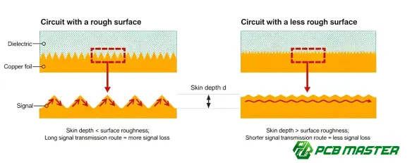
Higher conductor loss occurs with rougher copper surfaces because high frequency signals are forced to travel a longer, less uniform path.
At high frequencies the electrical current mainly flows near the surface of the copper, due to the skin effect. If the copper surface is rougher, the signal has more resistance which increases the insertion loss.
Benefits of a smoother copper surface are:
- Lower conductor loss
- Better signal integrity
- Better Delta-L performance
- More consistent high-frequency behavior
For example, two PCBs made on the same laminate may show different Delta-L results simply because one has ultra-low-profile copper and the other has standard rough copper foil.
Etching accuracy
Accurate PCB etching ensures the transmission line dimensions are as designed, which helps keep controlled impedance and reliable insertion loss measurements.
The width and spacing of the traces is determined by the etching process. If the traces are too narrow or too wide the impedance is altered, which impacts both signal reflections and insertion loss.
High etching accuracy provides:
- Stable impedance control
- Consistent transmission line geometry
- Better repeatability of measurements
- Improved manufacturing quality
In other words, if the over-etch reduces the trace width, the impedance may increase beyond the desired value and the Delta-L measurement will be different from the expected.
Trace width and spacing tolerance
The trace width and spacing should be kept tight to keep the target impedance and reduce variation between Delta-L measurements .
Controlled impedance is a function of the exact transmission line geometry. Small manufacturing variations may affect the electrical performance especially at high frequencies.
Good manufacturing control should include:
- Consistent trace width
- Uniform differential pair spacing
- Stable impedance over the full coupon
- Minimal variation between production lots
For example, a production lot with traces that are slightly wider than those in another lot could lead to a different measured insertion loss, even when the same PCB material is used. Tight fabrication tolerances improve product quality and Delta-L measurement consistency.
PCB thickness consistency
The thickness of the PCB needs to be consistent such that the impedance is consistent and the signal will travel across the Delta-L coupon in a predictable manner.
The distance between the signal layer and the reference plane is an important factor of controlled impedance . If the PCB thickness varies during manufacturing, the impedance and insertion loss can also vary.
Maintaining board thickness consistency helps to:
- Maintain target impedance
- Enhance signal integrity
- Boost measurement repeatability
- Minimize variation between manufactured panels
For example, if one part of the PCB is just a little thicker than another part, the transmission line impedance may be different, resulting in variation in insertion loss across otherwise identical coupons.
Process stability versus material performance
If your manufacturing process isn’t stable, you’ll never really know how well your PCB materials perform. Manufacturing variation can obscure the true performance of the material.
If the manufacturing process is different between test samples, the difference may not be attributed to the material itself. Delta-L testing is one of the main goals to compare the insertion loss of different PCB materials.
Some of the fabrications process variables that need to be held constant are:
- Trace width and spacing
- Copper thickness
- Surface roughness
- Lamination process
- Etching quality
- Drilling accuracy
- Plating consistency
For example, consider two Delta-L coupons made from different laminates. One coupon was made with tighter impedance control and smoother copper than the other coupon which had more process variation. Even though the two materials have similar electrical properties, the measured insertion loss may appear different.
For this reason, PCB manufacturers usually strive for the most consistent fabrication process possible when evaluating new materials. The Delta-L test, when applied to a stable manufacturing process, can separate the performance of the material from the variation of the process, leading to more reliable data for material qualification and validation of high speed PCBs.
What Is the Difference Between Delta-L 3.0 and Delta-L 4.0?
Delta-L 4.0 is designed for next generation high speed PCBs. The biggest difference is higher frequency measurements as well as a better coupon design. It has better probe launches, smaller probe pads, better via structures and tighter impedance control for more accurate insertion loss measurements.
As data rates increase, the effects of small impedance discontinuities become more significant. Delta-L 4.0 was developed to reduce these undesirable effects and provide accurate insertion loss measurements for advanced applications such as PCIe Gen5, PCIe Gen6 and 800G networking.
Supported frequency range
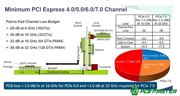
Delta-L 3.0 is typically used for measurements up to approximately 20 GHz, whereas Delta-L 4.0 extends the measurement range up to approximately 40 GHz.
The supported frequency range determines the types of high-speed interfaces that can be accurately evaluated. As signal frequencies increase, it becomes more difficult to measure the transmission line loss, reflections and impedance discontinuities.
General:
- Delta-L 3.0: Suitable for measurements up to approx. 20 GHz
- Delta-L 4.0: Suitable for measurements up to approx. 40 GHz
Delta-L 4.0 offers a higher frequency capability and is thus better suited for the evaluation of today’s ultra-high-speed PCB designs, where signal integrity requirements are much stricter than in previous generations.
Supported high-speed standards
Delta-L 4.0 supports newer high-speed communication standards that run at much higher data speeds than those typically targeted by Delta-L 3.0.
As interface speeds increase, the insertion loss of the PCB becomes a critical design parameter. Engineers need more accurate measurement methods to verify that the transmission lines meet the increasingly demanding channel requirements.
Typical applications include: Delta-L 3.0
- PCIe Gen3
- PCIe Gen4
- Legacy high-speed Ethernet designs
- Traditional networking equipment
- General high-speed PCB validation
Delta-L 4.0
- PCIe Gen5
- PCIe Gen6
- 400G Ethernet
- 800G Ethernet
- AI servers
- High-performance computing (HPC)
- Next-generation data center infrastructure
These newer applications require lower insertion loss and tighter impedance control, which is why Delta-L 4.0 is the preferred testing method.
Coupon structure differences
There are several improvements to the test coupon in Delta-L 4.0, to reduce measurement error, and better represent the actual performance of the PCB transmission line.
The overall measurement principle remains the same, but the coupon design has been refined to minimize reflections and impedance discontinuities.
Smaller probe pads
Delta-L 4.0 uses smaller probe pads than Delta-L 3.0.
Smaller pads help:
- Reduce impedance discontinuities
- Lower return loss
- Improve probe transitions
- Increase measurement accuracy
Because the probe pad is one of the first structures encountered by the signal, reducing its electrical impact improves the overall quality of the measurement.
Improved probe launch
The transition between the probe pads and the transmission line has been carefully optimized in Delta-L 4.0.
A smoother launch allows for:
- More continuous impedance
- Lower signal reflection
- Better repeatability
- Better measurement of insertion loss
This is especially important for frequencies over 20 GHz where even small discontinuities can have a noticeable effect on the results.
Better via optimization
Delta-L 4.0 puts more emphasis on the electrical effects of the vias.
Common optimization techniques are:
- Shorter via stubs
- Back drilling
- Via-in-Pad Plated Over (VIPPO)
- Improved via geometry
These improvements reduce high frequency reflections and help to ensure that the measured insertion loss represents the transmission line rather than the via structure.
Stricter impedance consistency
Delta-L 4.0 requires greater stringent impedance uniformity throughout the entire coupon.
Greater attention is given to:
- Trace width
- Trace spacing
- Copper thickness
- Dielectric thickness
- Ground reference continuity
- Manufacturing tolerances
The goal is to ensure that insertion loss differences are caused only by the additional transmission line length and not by local impedance variations.
Comparison table
Delta-L 4.0 builds on the Delta-L 3.0 measurement method by extending the frequency range and improving coupon design for next-generation high-speed applications.
| Feature | Delta-L 3.0 | Delta-L 4.0 |
|---|---|---|
| Typical frequency range | Up to ~20 GHz | Up to ~40 GHz |
| Target applications | Conventional high-speed PCBs | Next-generation ultra-high-speed PCBs |
| PCIe support | Up to approximately Gen4 | Gen5 and Gen6 |
| Ethernet support | Earlier high-speed Ethernet | 400G and 800G Ethernet |
| Probe pad design | Standard pads | Smaller optimized pads |
| Probe launch | Standard transition | Optimized low-reflection launch |
| Via design | Conventional optimization | Greater focus on back drilling and VIPPO |
| Impedance requirements | Controlled impedance | Stricter impedance consistency |
| Measurement accuracy | High | Higher at very high frequencies |
Why Delta-L 4.0 is required for PCIe Gen5, Gen6 and 800G applications
Delta-L 4.0 is required because modern high-speed interfaces operate at frequencies where even very small discontinuities can significantly impact signal quality.
Technologies such as PCIe Gen5, PCIe Gen6 and 800G Ethernet are transmitting data at very high speeds. At these frequencies signal loss is more and more pronounced and even minor variations in probe pads, vias or transmission line geometry can affect the measurement.
Delta-L 4.0 meets these challenges with:
- Higher frequency measurement capability
- Lower reflection coupon structures
- Better probe transitions
- Improved via performance
- Tighter impedance control
- More reliable insertion loss measurements
A coupon design that works well for PCIe Gen4, for example, may show too much reflection when tested at PCIe Gen6 frequencies. By optimizing the coupon structure and expanding the measurement range, Delta-L 4.0 delivers the accuracy needed to validate the most demanding high-speed PCB designs today.
As AI servers, cloud computing, and high-speed networking continue to evolve, Delta-L 4.0 has emerged as a key validation method for PCB manufacturers, material suppliers, and system designers engaged in the development of next-generation electronic products.
Where Is Delta-L Testing Used?
Delta-L testing is often used in applications where high speed signal transmission is needed. It can be used by engineers to test the insertion loss of a PCB, compare PCB material, and to make sure high speed circuit boards will meet signal integrity specifications before the product goes into mass production.
With the ongoing evolution of technologies such as AI, cloud computing, autonomous vehicles and high-speed communications, there is an increasing need for low-loss PCBs. Delta-L testing has emerged as an important verification method for PCB manufacturers, material suppliers and OEMs working on next-generation electronic products.
AI servers
Delta-L testing is critical to ensure signals are passed reliably in AI servers where massive amounts of data move between processors, memory, storage, and networking devices.
Modern AI servers have multiple high speed interfaces working simultaneously. Signals travel through long PCB traces between CPUs, GPUs, AI accelerators, memory modules and network cards. Excessive insertion loss may lead to signal quality degradation and affect overall system performance.
Delta-L testing is used widely to:
- Qualify low loss PCB materials
- Characterize high-speed transmission lines
- Improve signal integrity (SI)
- Facilitate PCIe Gen5 and Gen6 designs
- Validate high-speed manufacturing quality
For example, in designing an AI training server, engineers might use Delta-L testing to compare several PCB laminates to select the lowest insertion loss material for GPU interconnects.
Data center networking equipment
Delta-L tests data center networking equipment to ensure reliable high speed communication between servers, storage systems and network infrastructure.
Modern data centers process enormous amounts of information every second. Switches, storage systems, and network interface cards depend on high-speed PCB channels that must maintain low insertion loss over long transmission paths.
Delta-L testing benefits manufacturers:
- Verifies PCB channel performance
- Provides high frequency material comparison
- Validates manufacturing consistency
- Reduces signal degradation
- Increases network reliability
For example, engineers can use Delta-L testing to verify that the PCB meets insertion loss targets before releasing a new 800G network card.
High-speed switches and routers
Delta-L testing is used to validate PCB transmission lines that carry large amounts of network traffic in high-speed switches and routers.
There are many high-speed differential channels interconnecting processors, switch chips, memory and optical modules in enterprise switches and core routers. Such channels must maintain excellent signal integrity to support continuous data transmission.
Delta-L testing helps engineers:
- Accurately measure insertion loss
- Optimize PCB layouts
- Verify impedance-controlled routing
- Compare different PCB materials
- Reduce transmission errors
Accurate measurements of insertion loss are especially important as networking equipment continues to evolve from 100G to 400G and 800G Ethernet.
Telecommunications equipment
Delta-L testing is used on telecommunications equipment to check the quality of signals in high-frequency communication systems.
Telecommunication devices often operate over broad frequency ranges and must deliver stable performance under continuous operation. High insertion loss can reduce communication quality and system reliability.
Typical applications include:
- 5G and next-generation wireless infrastructure
- Optical communication equipment
- Base stations
- Microwave communication systems
- High-speed transmission modules
For example, a telecommunications equipment manufacturer could use Delta-L testing in the design process to verify that the PCB is capable of supporting high-frequency signals with minimal loss.
Automotive high-speed electronics
The Delta-L testing makes it possible to develop today’s vehicles with high speed electronic communication systems.
Modern vehicles are equipped with many more electronic systems than conventional vehicles . Advanced Driver Assistance Systems ( ADAS ) , infotainment , cameras , radar modules and high speed in-car networks all require reliable PCB signal transmission .
Delta-L testing aids automotive manufacturers to:
- Evaluate low-loss PCB materials
- Validate controlled impedance designs
- Enhance signal integrity
- Support reliable high-speed communication
- Increase product reliability
As automotive electronics increasingly utilize faster interfaces, the measurement of insertion loss is becoming more critical in the PCB validation process.
Aerospace electronics
Delta-L testing is used to validate the performance of high-frequency PCBs in mission-critical applications for aerospace.
Electronic systems used in aircraft, satellite and radar systems are often exposed to harsh environmental conditions and operate with high frequency signals.
Delta-L testing offers:
- Accurate measurement of insertion loss
- Reliable qualification of materials
- Consistent manufacturing verification
- Better signal integrity
- Higher confidence in long-term performance
For instance, engineers designing a radar control board can use Delta-L testing to guarantee that the PCB material selected will remain low in insertion loss across the target operating frequency range.
High-frequency PCB material qualification
elta-L testing is one of the more common methods for comparing and qualifying high frequency PCB materials.
New laminates are often tested by material suppliers and PCB manufacturers before going into production. Because Delta-L removes most measurement setup errors, it provides a reliable way to compare the electrical performance of different materials under the same test conditions.
Delta-L testing is commonly used to evaluate:
- Dielectric loss
- Overall insertion loss
- Manufacturing consistency
- Material-to-material performance
- Suitability for high-speed applications
For example, a PCB manufacturer may compare several low-loss laminates for an AI server project. Engineers can use the same Delta-L coupons to test each material to find out which laminate will give the lowest insertion loss without sacrificing manufacturing performance.
Due to its high accuracy and repeatability, Delta-L testing is the industry-standard method for qualifying PCB materials used in AI servers, data centers, telecommunications, automotive electronics, aerospace systems and other high-speed electronic applications.
How Should Delta-L Test Results Be Interpreted?
Look at the Delta-L test results for insertion loss per unit length, compare the measured insertion loss to the design goals, and determine if any excess insertion loss is due to the PCB material or the manufacturing process. Proper interpretation enables the engineer to confirm the PCB performance and identify potential improvements.
A Delta-L measurement is not a number. The engineers read the results with the PCB design specifications, material properties and manufacturing data to understand what the real electrical performance of the transmission line is.
Understanding insertion loss per unit length
Insertion loss per unit length is a measurement of the signal strength loss as it travels a certain length of PCB transmission line.
Delta-L testing reports insertion loss in units such as dB/in or dB/cm, which makes it easy to compare different PCB materials and designs without regard to the total trace length.
Generally:
- The lower the value of the insertion loss, the less energy is lost from the signal in transmission.
- The higher the insertion loss value, the faster the signal decays when traveling on the PCB.
For example:
- PCB Material A: 0.18 dB/cm
- PCB Material B: 0.25 dB/cm
Material A has less insertion loss under the same test conditions and is generally more suitable for high-speed applications where signal integrity is important.
Since the result is length normalized, engineers have a fair way to compare different PCB materials, manufacturing processes or transmission line designs.
Comparing measured values with design targets
Measured delta-L results should be compared to the insertion loss limits defined by the product design or applicable high-speed communication standard.
In most high-speed PCB projects, electrical performance objectives are established before the start of the manufacturing process. These objectives are derived from simulation results, industry standards, or system-level channel budgets.
Engineers usually evaluate Delta-L results by asking the following question:
- Does the measured insertion loss meet the design specification?
- Are the values the same as in the simulation?
- Are results from each production run similar?
- Is there sufficient performance margin to ensure safe operation?
For example, if the design goal is 0.20 dB/cm and the measured result is 0.18 dB/cm, the insertion loss requirement has been achieved; if the measured value is 0.27 dB/cm, engineers will need to investigate the PCB material, routing design, or manufacturing process before approving production.
The measurement results have to be compared with the predefined targets to assure that the PCB can work reliably in real world applications.
Identifying whether loss comes from materials or manufacturing
Delta-L results, manufacturing data and material specifications are used by engineers to help determine the source of insertion loss.
Higher than expected insertion loss does not necessarily indicate PCB material is poor, manufacturing variations can also increase signal loss.
Material-related causes are:
- Higher dissipation factor (Df)
- Higher dielectric constant (Dk)
- Rougher copper foil
- Lower-quality laminate
Manufacturing-related causes are:
- Trace width variation
- Incorrect trace spacing
- PCB thickness variation
- Copper plating differences
- Over-etching
- Poor impedance control
For example, if two Delta-L coupons are built with the same laminate and one coupon has a noticeably higher insertion loss, the difference is more likely due to manufacturing variation than material. Conversely, if two different laminates are fabricated using the same stable manufacturing process, then any consistent difference in insertion loss is more likely due to the material properties.
This comparison is useful for the engineers to decide to improve the fabrication process or to choose another PCB material.
Common reasons for unexpected test results
Unexpected Delta-L results are generally due to issues with the test set-up, coupon design, manufacturing consistency or material properties.
If the insertion loss measurement is very different to what is expected engineers should look at the entire testing process and not assume it is the PCB material that is at fault.
Typical causes are:
- VNA calibration error
- Poor probe contact
- Damaged or contaminated probe pads
- Coupon design differences between short and long traces
- Impedance discontinuities
- Excessive via stubs
- Trace width or spacing out of tolerance
- PCB thickness variations
- Higher than expected copper surface roughness
- Material properties different from design specification
A practical way to debug is to check each factor individually. The first check is calibration and measurement setup. The next is coupon design and quality of manufacture. Finally compare the measured material properties with the supplier’s specifications.
This systematic process helps engineers find the true source of the problem and ensures that Delta-L test results represent the performance of the PCB transmission line.
What Are the Advantages and Limitations of Delta-L Testing?
Delta-L testing is one of the most accurate ways to measure insertion loss in PCBs, making it a great choice for high-speed PCB validation and material comparison. However, it does require specialized equipment, well-designed test coupons and consistent manufacturing processes. Understanding the pros and cons of Delta-L testing helps engineers select the right testing method for their projects.
Advantages
Delta-L testing is very accurate, can help to reduce measurement errors, can be used for comparison of PCB materials and is accepted in the high speed PCB industry.
High measurement accuracy
Delta-L measures insertion loss accurately, because it only measures the extra loss of the extra length of the transmission line.
Instead of measuring a single PCB trace, Delta-L compares a short coupon with a long coupon that share the same structure. Since most external measurement errors appear in both coupons, they are largely canceled during the calculation.
This technique allows engineers to:
- Make more accurate insertion loss measurements
- Improve measurement repeatability
- Better characterize high speed PCB performance
For example, when qualifying a PCB for PCIe Gen6, even a small measurement error can affect design decisions.
Removes fixture and probe influence
Delta-L reduces the effects of probes, fixtures, connectors and other common measurement elements.
Direct insertion loss measurements include losses from the entire measurement path, not just the PCB transmission line. Delta-L removes most of these common influences by comparing two nearly identical coupons measured under the same conditions.
This allows you to:
- Minimize measurement uncertainty
- Make a fair comparison of different PCB samples
- Trust the end results
For example, while testing both coupons with the same probe and fixture, the majority of the common losses are eliminated in the Delta-L calculation and what is left is a better representation of the PCB trace itself.
Suitable for material comparison
Delta-L is a good way to compare the electrical performance of different PCB materials.
The test method removes errors from external measurements so any difference in insertion loss is more likely to be due to the actual properties of the PCB materials.
When two PCB laminates are processed the same way and tested using the same coupons, the material with the lower insertion loss will usually be selected for high-speed applications such as AI servers or data center network equipment.
Industry-recognized methodology
Delta-L has been proven to be an industry accepted method of insertion loss measurement in the PCB industry.
Many PCB manufacturers, laminate suppliers and OEMs use Delta-L testing during the product development and qualification stages because it provides consistent and repeatable results.
Delta-L is used in a variety of applications such as:
- High speed PCB validation
- Material qualification
- Manufacturing process evaluation
- Signal integrity verification
- Research and product development
The industry’s use of delta-L makes it easy for companies to compare test results using a common measurement methodology.
Limitations
Delta-L testing is very good, but it is not the right answer for every situation. The method requires special coupon design, sophisticated equipment, consistent manufacturing, and should be used in conjunction with other signal integrity evaluation techniques.
Requires carefully designed coupons
Delta-L testing is only as good as the test coupons used.
Long and short coupons should be the same except for the length of the transmission line. Any small difference in pad size, via structure, routing or impedance can affect the measured results.
Engineers must be careful to consider:
- Geometry of the transmission line
- Design of the probe pad
- Configuration of the vias
- Ground reference
- Controlled impedance
A poorly designed coupon will degrade the accuracy of the entire measurement.
High equipment cost
Specialized equipment is required for Delta-L testing, and this equipment can be expensive to purchase and operate.
A complete Delta-L measurement system typically consists of:
- A high performance Vector Network Analyzer (VNA)
- High frequency probes
- Calibration standards
- Precision fixtures
- Professional analysis software
Beyond the cost of the equipment, it takes trained engineers to perform the calibration, operate the instruments and interpret the measurement results. That’s why Delta-L testing is generally performed by experienced PCB manufacturers, test labs or material suppliers.
Sensitive to manufacturing consistency
mall variations in manufacturing can cause large variations in Delta-L.
Delta-L Quantifies very small insertion loss variations Small manufacturing variations can affect the final reading.
Some important manufacturing factors are:
- Trace width tolerance
- Trace spacing tolerance
- Copper thickness
- Copper surface roughness
- PCB thickness
- Lamination quality
- Etching tolerance
For example, if one run has wider traces than another, the insertion loss reading might be different, even if the same PCB material is used.
Cannot replace complete channel validation
Delta-L is a measure of the insertion loss of a PCB transmission line, not a measure of the performance of the entire high-speed communication channel.
The entire signal path in most applications consists of:
- PCB traces
- Connectors
- Packages
- Sockets
- Cables
- Integrated circuits
- Other interconnect structures
While Delta-L is an accurate measure of the PCB insertion loss, engineers still need to perform other signal integrity analyses, such as eye diagram testing, channel simulation, return loss analysis, and bit error rate (BER) testing, to assess the overall system performance.
For example, a PCB may achieve excellent Delta-L results but still fail system-level testing because of poor connector performance or excessive channel reflections elsewhere in the signal path.
For this reason, Delta-L testing should be viewed as one important part of a comprehensive high-speed PCB validation strategy rather than a replacement for complete channel validation.

How Can PCB Manufacturers Improve Delta-L Performance?
PCB manufacturers can assist Delta-L performance by minimizing insertion loss and controlling manufacturing variation. This is achieved through the deployment of low-loss materials, stringent impedance control, smoother copper surfaces, optimized via designs, stable fabrication processes, and Delta-L coupons that meet the latest specifications.
The Delta-L test measures the electrical performance of a PCB transmission line so the PCB material and manufacturing process both have an impact on the end results. Improving these factors allows manufacturers to produce low insertion loss, better signal integrity and more consistent high-speed PCBs.
Select low-loss PCB materials
Choosing low-loss PCB materials is one of the best ways to enhance Delta-L performance.
When a signal passes through any PCB material, a small amount of the signal energy is absorbed. Low dissipation factor (Df) and stable dielectric constant (Dk) materials reduce the loss of this energy which leads to lower insertion loss.
Manufacturers should seek:
- Low Df, to reduce dielectric loss
- Stable Dk over the range of operating frequencies
- Good thermal and mechanical stability
- Proven performance in high-speed applications
For example, AI servers and 800G networking equipment typically use special low-loss laminates, instead of standard FR-4, due to their improved signal integrity at very high data rates.
Improve impedance control capability
Proper impedance control reduces reflections and ensures that the Delta-L measurements accurately reflect the PCB transmission line.
To control the impedance, the transmission line geometry has to be consistent during the manufacturing process .
Manufacturers must tightly control the following:
- Trace width
- Trace spacing
- Dielectric thickness
- Copper thickness
- Layer alignment
Advanced impedance simulation and process control will help keep the final PCB close to its target impedance like 85 Ω or 100 Ω differential.
For example, if trace widths vary from production panel to production panel, insertion loss measurements may vary as well, making it difficult to accurately compare PCB materials.
Reduce copper roughness
Smoother copper surfaces will reduce conductor loss and improve high frequency signal transmission.
At high frequencies the skin effect causes the electrical current to flow mainly along the outer surface of the copper conductor. Rough copper increases the path the current must travel, thus increasing resistance and insertion loss.
Manufacturers can optimize Delta-L performance by:
- Using ultra-low-profile (ULP) copper foil
- Controlling surface treatment processes
- Choosing copper foils formulated for high-speed PCBs
- Maintaining consistent copper surface quality
For instance, the use of ultra-low-profile copper foil instead of standard rough copper foil can drastically reduce insertion loss in high-frequency PCB design.
Optimize via structures
The short answer: Well designed vias will reduce the signal reflections and will reduce the extra insertion loss.
Vias are often a necessary evil in many PCB designs, but can cause impedance discontinuities and unwanted resonance if not properly optimized.
Common optimization techniques include:
- Reducing stub length
- Back drilling
- Via-in-Pad Plated Over (VIPPO)
- Optimizing anti-pad geometry
- Symmetrical differential vias
For example, back drilling long via stubs can improve high-frequency performance by reducing signal reflections, especially for PCIe Gen6 and 800G applications.
Maintain stable manufacturing processes
Stable manufacturing processes are required for consistent and repeatable Delta-L results.
Insertion loss can change due to manufacturing variations , even if the same PCB material is used .
Manufacturers must tightly control the following:
- Lamination
- Drilling
- Plating
- Etching
- Surface finishing
- Thickness control
- Quality inspection
For example, if the thickness of the copper plating varies significantly from batch to batch, then the electrical characteristics of the transmission line may also vary. Stability in process control can help ensure that measured differences are caused by true material performance and not due to manufacturing variation.
Design coupons according to the latest Delta-L specifications
Using the latest Delta-L coupon specs will improve the accuracy of your measurements and will be compatible with modern high speed PCB testing.
The design requirements for coupons for the newer Delta-L specifications are more stringent with the increasing communication speeds to minimize the measurement uncertainty.
Modern Delta-L coupon design usually consists of:
- Smaller probe pads
- Optimized probe launches
- Improved via structures
- Continuous ground reference planes
- Tighter impedance control
- Better differential pair symmetry
For example, Delta-L 4.0 coupons are optimized for measurements up to about 40 GHz and are suitable for validating PCIe Gen5, PCIe Gen6, and 800G Ethernet designs. By following the latest coupon design guidelines, PCB manufacturers can generate more accurate, repeatable, and industry-recognized Delta-L test results while achieving the performance requirements of next-generation high-speed electronic products.
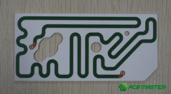
Conclusion: Why Has Delta-L Become the Preferred Method for PCB Insertion Loss Measurement?
As high-speed electronics continue to evolve, Delta-L testing has become one of the most reliable methods of PCB insertion loss measurement. Delta-L measures two transmission lines with the only difference being length and reduces measurement errors introduced by probes, fixtures and vias, providing a better picture of the PCB itself. To obtain reliable results, well designed test coupons, controlled impedance, optimized via structures, and consistent manufacturing processes are required.
As AI servers, data centers, PCIe Gen6 and 800G networking demand higher bandwidth going forward, accurate insertion loss measurement will become even more critical. As PCB technologies continue to evolve, Delta-L testing will continue to be an important tool to verify materials, manufacturing quality and overall signal integrity.
As these challenges grow, choosing the correct test method is as critical as partnering with an experienced PCB manufacturer. PCBMASTER offers customers state-of-the-art PCB fabrication, rigid impedance control and high speed PCB manufacturing expertise to help build reliable, low loss circuit boards that can meet the performance requirements of next generation electronic applications.
FAQs
What does Delta-L measure in a PCB?
Delta-L is a method to measure the insertion loss per unit length of a PCB transmission line . Instead of measuring one trace , it measures two almost identical test coupons with slightly different trace lengths . The difference in insertion loss is calculated and divided by the length difference ( ΔL ) to find out how much signal attenuation would occur over a certain distance , usually expressed in dB/in or dB/cm .
Is Delta-L testing the same as insertion loss testing?
No. Delta-L testing is not a different electrical parameter, but a specific technique for measuring insertion loss. Both techniques measure insertion loss, but Delta-L uses a differential comparison of a long coupon and a short coupon to remove common measurement errors due to probes, connectors, fixtures and vias. This provides a more accurate representation of the PCB transmission line itself than a direct insertion loss measurement.
What is the difference between Delta-L 3.0 and Delta-L 4.0?
So the main difference is that Delta-L 4.0 supports higher frequency measurements and more advanced high-speed PCB designs. Compared with Delta-L 3.0, Delta-L 4.0 extends the measurement range from approximately 20 GHz to 40 GHz, uses smaller probe pads, optimized probe launches, improved via structures, and stricter impedance control. These enhancements make Delta-L 4.0 suitable for next-generation applications such as PCIe Gen5, PCIe Gen6, 400G Ethernet, and 800G Ethernet.
Why does Delta-L testing use two different trace lengths?
Delta-L testing uses a short coupon and a long coupon because the difference between the two measurements represents only the additional loss caused by the extra transmission line length. Since both coupons use the same probes, fixtures, connectors, and via structures, most common measurement errors cancel out during the calculation. This differential measurement method provides better accuracy and repeatability of insertion loss results than direct measurement of a single transmission line.
Can Delta-L testing evaluate PCB materials?
Yes, delta-L testing is a standard method to test the electrical performance of PCB materials, particularly in high speed and high frequency applications. Engineers compare insertion loss under the same test conditions for various laminates to find materials with lower signal loss. But for the measurements to be meaningful in terms of the material performance, the manufacturing process has to be consistent. Variations in trace dimensions, copper roughness, PCB thickness, or impedance control can all influence the measured insertion loss, and so it becomes difficult to distinguish the differences in the material property from process variation.
About the Author

Carol Luo
PCB Design EngineerI'm Carol, a PCB Engineer at PCBMASTER with experience in PCB design and manufacturing engineering since 2018. I focus on translating engineering requirements into reliable PCB solutions, with expertise in stack-up design, material selection, and design-for-manufacturing (DFM). I share practical engineering insights from real-world PCB design and production experience.
Visit Carol Luo's Profile
