PCB Design Basics for Electronics Engineers: Key Principles Explained
PCB design is the foundation of every electronic device, forming the backbone that connects and powers all components. As a seasoned PCB and PCBA supplier, PCBMSTER understands that the quality of PCB design directly impacts the performance, reliability, and longevity of electronic products. Without a well-designed PCB, even the most advanced components won’t function properly, leading to malfunctioning devices or costly failures.
For electronics engineers, mastering PCB design is not just about understanding how components connect; it's about creating a reliable, efficient, and durable circuit board. From ensuring the right material choice to optimizing the layout for signal integrity, every decision in the design process plays a crucial role in the final product. This article will guide you through the essential principles of PCB design, helping you grasp the fundamentals needed for designing high-performance circuit boards that meet the demands of modern electronics.
What Are the Key Components of a PCB?
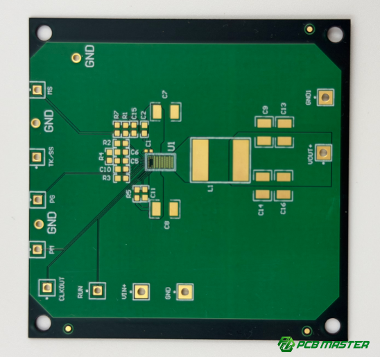
The key components of a PCB include the schematic diagram, component selection, PCB layers, pads, traces, vias, and efficient component placement, all of which work together to ensure the circuit's functionality and reliability.
Schematic Diagram and Component Selection
Before starting a PCB design, it's essential to understand the schematic diagram. This diagram shows how all the components will connect on the board. Selecting the right components is crucial. Each electronic component, such as resistors, capacitors, and microchips, must be chosen carefully based on the circuit's function. Components need to be compatible with each other, and their specifications (like voltage, current, and power ratings) must match the requirements of the design. A wrong component can lead to malfunction, inefficiency, or even damage to the circuit.
PCB Layers
The number of layers in a PCB affects both its complexity and cost. A single-layer PCB has one conductive layer, making it simple and cost-effective for basic circuits. However, as the circuit design becomes more complex, multi-layer PCBs are necessary. Multi-layer PCBs provide more space to place traces and components, allowing for more complex and dense circuits. While multi-layer designs are more expensive, they are essential for high-performance applications such as smartphones, computers, and medical devices.
Pads, Traces, and Vias
Pads, traces, and vias are the lifeblood of any PCB. Pads are the small copper areas where components are soldered. Traces are the conductive paths that connect the pads, allowing electricity to flow between components. Vias are small holes that allow traces on different layers of a multi-layer PCB to connect. The design and layout of these elements directly influence the stability and performance of the PCB. Poorly placed traces or vias can lead to signal interference, overheating, or even circuit failure.
Component Placement
Efficient component placement is vital for the performance and manufacturability of a PCB. Proper placement reduces the chance of signal interference, minimizes noise, and ensures the assembly process goes smoothly. Components should be placed to keep the signal path as short as possible, reducing resistance and inductance. Additionally, components that generate heat should be placed with enough space for heat dissipation. An effective layout also considers how the components will be soldered during assembly, ensuring ease of production. Proper placement ultimately results in a functional and reliable PCB.
How Do You Start a PCB Design Project?
To start a PCB design project, first define the product's design requirements, select the appropriate PCB design software, and set design constraints such as size, material, and power requirements to ensure functionality and manufacturability.
Design Requirements and Specifications
Before beginning a PCB design, it is essential to understand the product's requirements. This includes factors such as voltage, current, environmental conditions, and the overall function of the circuit. For example, if you're designing a PCB for an industrial application, it must be able to withstand higher temperatures and vibrations compared to one used in a consumer device. By defining these requirements early on, you set clear design goals that guide decisions throughout the process, from selecting components to determining the PCB’s size and power capacity.
Choosing the Right PCB Design Software
There are many PCB design tools available today, each offering different features and capabilities. Popular choices include Eagle, KiCad, and Altium Designer. Eagle is great for beginner to intermediate projects, offering an intuitive interface and extensive online support. KiCad is an open-source option, perfect for those with a tighter budget or who want to customize their designs. Altium Designer is a high-end, professional tool that excels in complex, multi-layer PCB designs and integrates well with other engineering software. As a professional PCB supplier, PCBMSTER offers technical support to help guide you in choosing the best software based on your project needs.
Setting Design Constraints
Setting design constraints is crucial for ensuring that your PCB is manufacturable and functional. These constraints include the board’s size, the type of materials used, and power requirements. For instance, if your design needs to handle high power, you may need thicker copper traces or special materials to reduce heat. By clearly defining these constraints, you can avoid issues later in the manufacturing process and ensure that the design meets both performance and production standards. Constraints also help when it comes to complying with regulatory standards, such as those required for medical or automotive devices.
What Are the Key Design Considerations for Effective PCB Design?
The key design considerations for effective PCB design are maintaining signal integrity, ensuring efficient thermal management, and optimizing power distribution and grounding to enhance stability and performance.
Signal Integrity
Signal integrity is crucial, especially in high-frequency circuits. It refers to the quality and reliability of the electrical signals traveling through the PCB. Poor signal integrity can lead to problems like interference, noise, and crosstalk, which may cause the circuit to behave unpredictably or fail completely. To maintain signal integrity, it’s important to minimize the effects of electrical noise and interference. Techniques like keeping trace lengths as short as possible, using proper grounding, and adding shielding can help reduce signal loss and ensure clean, reliable signals. For example, in high-speed communication circuits like those in smartphones, maintaining signal integrity is key to ensuring data is transmitted accurately.
Thermal Management
Effective thermal management is essential to prevent overheating of components, which can lead to malfunction or damage. As electronic devices get smaller and more powerful, managing heat becomes more challenging. In PCB design, this involves ensuring there is sufficient heat dissipation through methods like using heat sinks, thermal vias, and spreading the heat evenly across the board. For instance, high-power devices such as power amplifiers or processors require careful thermal analysis to ensure they don’t overheat. At PCBMSTER, we provide expert thermal analysis and design recommendations to ensure your PCBs can handle the heat, leading to stable and reliable performance.
Power Distribution and Grounding
Power distribution and proper grounding are fundamental to the stability and performance of a PCB. A good power distribution system ensures that each component gets the right amount of voltage and current, preventing voltage drops or power surges that could damage sensitive components. Similarly, proper grounding minimizes electrical noise and interference, helping to stabilize the overall system. In complex PCBs, multiple ground planes and dedicated power planes are often used to optimize performance. For example, in a high-performance PCB, having a solid ground connection can prevent unwanted signals from interfering with the circuit, improving overall stability.
How Do You Lay Out PCB Traces and Components?
To lay out PCB traces and components effectively, calculate trace widths based on current requirements, optimize trace routing by minimizing length and avoiding sharp angles, and place components strategically for functionality, heat dissipation, and ease of assembly.
Trace Width Calculation
Trace width is crucial for ensuring your PCB can safely handle the required current without overheating or causing instability. The width of a trace is directly related to the amount of current it will carry. To calculate the correct width, you need to consider the current requirement, the copper thickness, and the acceptable temperature rise. A narrower trace can overheat if too much current passes through it, leading to potential damage or failure. For example, if you are designing a PCB for a high-power device, like a motor controller, wider traces will be necessary to avoid excessive heat buildup. Using online calculators and standards like IPC-2221 can help determine the optimal trace width for your design.
Trace Routing Optimization
To ensure stable signal transmission and reduce signal interference, it’s important to optimize the trace routing on your PCB. Shorter traces reduce the risk of signal loss and delay, ensuring faster and more reliable performance. Sharp turns in traces should be avoided, as they can cause impedance mismatch and signal reflection, leading to errors in signal transmission. Instead, use gentle curves or 45-degree angles to route traces. For example, in high-speed digital circuits like those in computers, careful routing ensures signals are transmitted cleanly and without interference. A well-planned trace routing is crucial for maintaining signal integrity, especially for high-frequency designs.
Component Placement Tips
Efficient component placement is essential for the overall performance and manufacturability of a PCB. When placing components, it’s important to consider their function, heat dissipation requirements, and ease of assembly. For instance, components that generate a lot of heat, like voltage regulators or power transistors, should be spaced to allow for proper airflow and cooling. Additionally, placing components that need to interact closely, such as the processor and memory, near each other can reduce trace lengths and improve performance. Proper component placement not only enhances functionality but also simplifies the manufacturing process, reducing the chances of errors during assembly.
How Do You Ensure PCB Design Compatibility with Manufacturing?
To ensure PCB design compatibility with manufacturing, apply Design for Manufacturability (DFM) principles, perform Design Rule Checks (DRC) using specialized software, and use panelization to reduce production costs and improve efficiency.
Design for Manufacturability (DFM)
Design for Manufacturability (DFM) is a key principle to ensure that your PCB design is not only functional but also easy and cost-effective to produce. By following DFM guidelines, you can avoid common manufacturing issues such as component misalignment, insufficient trace width, or placement errors. For example, if a design has overly small traces or tight spacing, it may be difficult to produce or result in manufacturing defects. As a PCB and PCBA manufacturer, PCBMSTER emphasizes the importance of DFM to minimize production delays and avoid costly revisions, ensuring that your design meets both performance and manufacturing standards.
Design Rule Check (DRC)
A Design Rule Check (DRC) is a crucial step in the PCB design process that helps ensure the design meets all manufacturing constraints. DRC uses specialized software tools to verify that your design complies with key parameters such as trace width, spacing, hole sizes, and layer alignment. By running DRC checks, you can identify potential issues before the design goes into production, saving both time and money. For instance, DRC can detect errors like trace widths that are too small for the intended current or vias that are too close to pads. It ensures your PCB design is ready for efficient and error-free manufacturing.
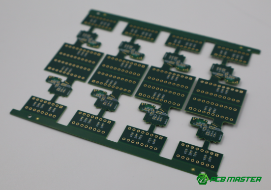
Panelization Design
Panelization is a process that involves grouping multiple smaller PCBs into one larger panel for manufacturing. This technique helps reduce production costs by optimizing the use of the board area and streamlining the manufacturing process. Once the individual PCBs are manufactured, the larger panel is cut into smaller, individual boards. This is especially useful for designs with small or medium-sized PCBs that can be efficiently arranged on a larger panel. For example, a batch of simple sensor boards can be panelized to lower the cost per unit and increase the efficiency of the PCB fabrication process.
How Do You Validate a PCB Design?
To validate a PCB design, perform electrical testing to check for short circuits or open circuits, conduct thermal testing to ensure components stay within safe temperature limits, and create prototypes for iterative testing and refinement before final production.
Electrical Testing
Electrical testing is essential to verify that your PCB design functions as intended. This testing checks for issues like short circuits (when two conductive paths mistakenly connect) or open circuits (when a path is broken). After the design is complete, engineers typically run circuit simulations to predict how the PCB will behave under real conditions. They also create a physical prototype of the PCB and perform live testing to ensure all connections are correct and the board works properly. For example, if you're designing a power supply PCB, electrical testing ensures that the voltage levels are stable and all components are functioning correctly before mass production.
Thermal Testing
Thermal testing assesses how well the PCB handles heat during operation. Electronic components generate heat, and if the temperature rises too high, it can damage the components or reduce their lifespan. During thermal testing, the PCB is tested under load conditions to measure the temperature of critical components, like voltage regulators or processors. If the temperature exceeds safe limits, adjustments are made to the design, such as improving heat dissipation through larger copper areas or adding heat sinks. For instance, in high-performance computing or power electronics, thermal testing is crucial to ensure that the PCB can operate safely without overheating.
Prototyping and Iterative Testing
Prototyping is a crucial step in PCB validation. It involves creating a physical version of the PCB based on the design, allowing engineers to check the board’s functionality in real-world conditions. This prototype is then tested and iterated on—any issues found during testing are addressed, and design adjustments are made. This iterative process helps ensure that the final product is reliable and performs as expected. For example, in the development of consumer electronics, prototypes undergo multiple rounds of testing to refine the design and fix any unforeseen issues before full-scale production.
What Are Common Challenges in PCB Design, and How Can You Avoid Them?
Common challenges in PCB design include signal degradation in high-speed circuits, the complexity of multi-layer designs, and component misalignment; these can be avoided by using high-quality materials, careful routing, working closely with manufacturers, and ensuring precise component placement and alignment.
High-Speed Circuit Design
High-speed circuits are especially vulnerable to signal degradation and electromagnetic interference (EMI) , which can lead to malfunctioning or poor performance. To avoid these issues, it is important to use high-quality materials, such as low-loss substrates and properly shielded traces. Additionally, precise routing is essential to reduce the distance signals travel and minimize interference. For example, in a high-speed data transfer circuit like USB or HDMI, carefully managing the trace width, spacing, and routing paths can significantly improve signal integrity. By following these best practices, you can ensure that your high-speed circuits perform reliably without signal loss or interference.
Complexity of Multi-Layer PCBs
Multi-layer PCBs provide more room for complex circuits, but their design and manufacturing are more challenging. The increased number of layers and interconnections can lead to issues like poor layer alignment or manufacturing defects if not handled properly. To avoid these problems, it’s important to work closely with your PCB manufacturer and ensure that the design is compatible with the intended production process. At PCBMSTER, we specialize in multi-layer PCB design and manufacturing, ensuring that every layer aligns correctly and the final board performs as expected. Proper planning and coordination between design and manufacturing teams are key to avoiding costly mistakes in multi-layer designs.
Component Tolerances and Alignment Issues
Precise component placement and alignment are essential for ensuring the PCB functions correctly and can be assembled efficiently. Any misalignment can lead to issues such as soldering problems or electrical malfunctions. To avoid these challenges, it's crucial to use high-precision equipment during the design phase and in the manufacturing process. At PCBMSTER, we utilize advanced machinery to ensure every component is placed accurately. Properly defining the tolerance levels for each component and ensuring that the design accommodates these specifications can prevent misalignment and ensure that the final product is assembled smoothly and without errors.
Conclusion
Mastering PCB design principles is crucial to building reliable and stable circuit boards. As a professional PCB and PCBA supplier, PCBMSTER understands that high-quality design is the foundation of any successful product. By gaining a strong understanding of the fundamentals of PCB design, engineers can not only improve their design efficiency but also ensure the stability and reliability of their boards. This knowledge helps avoid costly mistakes and reduces production errors, ultimately leading to better-performing electronics. We encourage every electronics engineer to continue learning and improving their design skills. Working together with PCBMSTER, you can explore innovative solutions, tackle new challenges, and create even more advanced and reliable PCBs. With the right design knowledge and collaboration, the possibilities are endless.
FAQs
1. What Are the Most Important Principles in PCB Design?
The most important principles in PCB design are signal integrity, thermal management, and power distribution. Signal integrity ensures that electrical signals are transmitted cleanly and without distortion, which is especially crucial in high-speed circuits. Poor signal integrity can lead to malfunction or errors in data transmission. Thermal management is critical for preventing overheating, which can cause components to fail. Proper heat dissipation techniques, such as using heat sinks and optimizing the layout for better airflow, are essential to maintaining the longevity of the PCB. Power distribution ensures that each component on the PCB receives a stable voltage and current, which helps prevent power surges or voltage drops that could damage sensitive components. Together, these principles ensure that the PCB operates reliably and efficiently in various applications.
2. How Can I Avoid Common Mistakes in PCB Design?
To avoid common mistakes in PCB design, it’s important to use Design Rule Checks (DRC) to ensure that your design complies with the manufacturing requirements. DRC tools are integrated into most PCB design software, and they check for issues like trace width violations, spacing errors, and unconnected pads. Running these checks before production helps identify design flaws that might cause issues during manufacturing. Additionally, performing prototype testing is critical. Prototyping allows you to test the physical PCB to identify any potential functional issues before mass production. Iterative testing and modifications will help ensure the final design is free of errors, reliable, and ready for full-scale production.
3. What PCB Design Software Do Electronics Engineers Commonly Use?
Some of the most commonly used PCB design software tools include Eagle, KiCad, and Altium Designer. Eagle is favored by many hobbyists and small-scale engineers due to its user-friendly interface and affordability. It’s ideal for simpler designs and is often used for educational purposes. KiCad, an open-source software, is popular for more advanced designs and offers a robust feature set, making it a great choice for those with limited budgets. Altium Designer, on the other hand, is a professional-grade software with advanced capabilities, ideal for complex, high-performance PCB designs. It is widely used by industry professionals for large-scale and intricate designs due to its powerful tools for simulation, 3D modeling, and collaboration.
4. What Is the Role of Thermal Management in PCB Design?
Thermal management is crucial in PCB design to prevent overheating, which can lead to component failure or reduced performance. As electronic devices become smaller and more powerful, the amount of heat generated by components increases. Without proper thermal management, excessive heat can damage the PCB and its components. Effective thermal management involves designing the PCB layout to minimize heat buildup, using heat sinks, and selecting materials with good thermal conductivity. Additionally, employing techniques like thermal vias or increasing the board’s copper thickness can help spread the heat more evenly across the surface. This ensures that components operate within their optimal temperature range, thereby extending their lifespan and improving the overall reliability of the circuit.
5. How Can I Ensure My PCB Design Will Be Successfully Manufactured?
To ensure your PCB design can be successfully manufactured, you need to follow Design for Manufacturability (DFM) principles. DFM involves designing the PCB in a way that simplifies the manufacturing process while minimizing potential errors. This includes ensuring that the design meets the capabilities of the PCB fabrication process, such as trace width, hole sizes, and component placement. Additionally, ensuring the design is not overly complex can help avoid production difficulties, reduce costs, and speed up manufacturing. Regularly conducting DFM reviews with your manufacturer can help address any potential issues early in the design phase, ensuring that your PCB can be fabricated without complications. Following these practices can help you avoid costly reworks and delays during production.
About the Author

Carol Luo
PCB Design EngineerI'm Carol, a PCB Engineer at PCBMASTER with experience in PCB design and manufacturing engineering since 2018. I focus on translating engineering requirements into reliable PCB solutions, with expertise in stack-up design, material selection, and design-for-manufacturing (DFM). I share practical engineering insights from real-world PCB design and production experience.
Visit Carol Luo's Profile