


What Are Castellated Holes in PCB Design? Benefits, Applications and Manufacturing Guide
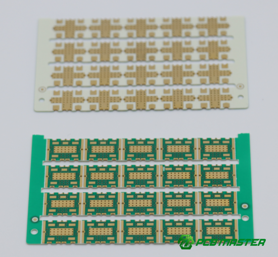
Castellated holes, also known as PTH half holes, are plated through-holes that are cut along the edge of a PCB, creating a semi-circular copper-plated opening. They are widely used in wireless modules, IoT devices, embedded systems, and compact electronic products where reliable board-to-board connections are required. By allowing a PCB module to be soldered directly onto a host board, castellated holes eliminate the need for connectors, reduce assembly costs, save space, and improve integration density. As a professional PCB and PCBA manufacturer, PCBMASTER frequently produces castellated-hole PCBs for high-density and high-reliability electronic applications.
What Is a PTH Half Hole (Castellated Hole)?
A PTH half hole, commonly referred to as a castellated hole, is created by drilling and plating a through-hole and then routing through the center of the hole along the PCB edge.
The result is a series of half-circle plated holes located on the board edge, functioning as solderable electrical and mechanical connection points.
Typical Applications
· Wi-Fi modules
· Bluetooth modules
· GPS modules
· RF communication modules
· IoT devices
· Sensor modules
· Embedded control boards
· Industrial communication systems
Key Functions of Castellated Holes in PCB Design
1. Enable Board-to-Board Module Connections
The primary purpose of castellated holes is to allow a PCB module to be mounted directly onto another PCB.
Instead of using:
· Pin headers
· Socket connectors
· Wire harnesses
the module can be soldered directly onto pads on the main board.
Benefits
· Lower assembly cost
· Reduced component count
· Improved reliability
· Faster manufacturing process
This approach is commonly used in wireless communication modules where compact integration is essential.
2. Support High-Density Electronic Designs
Space is often the most valuable resource in modern electronics.
Castellated holes eliminate bulky connectors and allow modules to occupy only their actual PCB footprint.
Advantages
| Design Factor | Traditional Connector | Castellated Hole Design |
| Board Space | High | Low |
| Assembly Height | Higher | Lower |
| Component Count | More | Less |
| Manufacturing Cost | Higher | Lower |
| Reliability | Good | Excellent |
This makes castellated-hole PCBs ideal for:
· Wearable electronics
· Portable devices
· Smart home products
· Medical electronics
· Industrial IoT equipment
3. Simplify Module Manufacturing and Assembly
Manufacturers can produce modules separately and test them independently before final assembly.
The verified module is then soldered onto the host PCB during standard SMT assembly.
Benefits include:
· Easier inventory management
· Reduced assembly complexity
· Higher production efficiency
· Better quality control
4. Facilitate Testing and Programming
Castellated holes can also serve as:
· Programming interfaces
· Debug ports
· Test access points
During development and manufacturing, engineers can test the module independently before integrating it into the final product.
This significantly reduces troubleshooting time and production risks.
5. Improve Electrical Performance
Compared with cable-based interconnections or certain connector solutions, castellated-hole connections provide:
· Shorter signal paths
· Lower contact resistance
· Better signal integrity
· Reduced EMI risk
This is particularly important for:
· RF modules
· High-speed digital circuits
· Communication equipment
· Automotive electronics
Important Design Considerations for Castellated Holes
Hole Position Relative to Board Edge
The hole center must be precisely positioned relative to the PCB outline.
Typical recommendations:
· Hole edge flush with PCB edge
· Small manufacturing allowance of 0.1–0.2 mm when required
Accurate positioning ensures proper formation of the castellated structure after routing.
Pad Size Optimization
Castellated-hole pads should generally be larger than standard plated through-hole pads.
Recommended practice:
· Extend the pad beyond the board edge
· Provide sufficient soldering area
· Improve solder joint reliability
Larger pads help increase both electrical conductivity and mechanical strength.
Proper Pitch and Spacing
Spacing between adjacent castellated holes must meet assembly requirements.
Insufficient spacing can cause:
· Solder bridging
· Short circuits
· Reduced manufacturing yield
PCB designers should follow the capabilities specified by their PCB manufacturer.
Manufacturing Challenges and Considerations
Drilling and Routing Sequence
The typical manufacturing process is:
1. Drill holes
2. Copper plate holes
3. Apply surface finish
4. Route board outline
5. Create castellated edges
Because routing cuts through plated holes, special process control is required to prevent copper peeling or edge damage.
Plating Quality
A high-quality castellated hole should have:
· Smooth copper walls
· Uniform plating thickness
· No cracks
· No delamination
At PCBMASTER, advanced AOI inspection and multi-stage quality control help ensure consistent plating quality for castellated-hole PCBs.
Routing Precision
Castellated holes require highly accurate CNC routing.
Poor routing accuracy may lead to:
· Uneven half holes
· Damaged copper walls
· Solderability issues
High-precision manufacturing equipment is essential for maintaining product consistency.
Assembly and Soldering Considerations
Stencil Design
Accurate stencil aperture design is critical.
Too much solder paste may cause:
· Bridging
· Excess solder
Too little solder paste may result in:
· Weak joints
· Open connections
A balanced stencil design ensures reliable solder formation.
Reflow Soldering Profile
Castellated-hole modules require sufficient thermal energy during reflow soldering.
Engineers should optimize:
· Preheat temperature
· Soak time
· Peak temperature
· Cooling rate
This helps achieve complete solder wetting and strong interconnections.
Mechanical Strength
Although castellated-hole joints provide reliable electrical connections, they generally offer less mechanical strength than fully inserted through-hole components.
Avoid using castellated-hole connections in areas subjected to:
· Frequent vibration
· Mechanical shock
· High insertion force
Additional support structures may be required for harsh environments.
Reliability Considerations
Surface Finish Selection
Because castellated holes are exposed at the PCB edge, surface finish selection is critical.
Recommended finishes include:
· ENIG (Electroless Nickel Immersion Gold)
· OSP (Organic Solderability Preservative)
These finishes improve:
· Corrosion resistance
· Solderability
· Long-term reliability
Rework and Repair Risks
Repeated soldering cycles may weaken castellated-hole pads.
When designing modules, engineers should consider:
· Rework allowances
· Pad reinforcement
· Thermal management
This helps reduce the risk of pad lifting during repair operations.
PCBMASTER's Expertise in Castellated Hole PCB Manufacturing
As a professional PCB and PCBA manufacturer, PCBMASTER provides complete support for castellated-hole PCB projects, from engineering review to mass production.
Why Engineers Choose PCBMASTER
Capability PCBMASTER Advantage Quality System ISO 9001, IATF 16949, UL Certified Engineering Support Free DFM Review Production Capacity HDI, Rigid-Flex, RF, FPC, Metal Core PCB Quality Assurance 100% Electrical Testing Delivery Performance 99.59% On-Time Delivery Technical Service 24/7 Engineering Support Manufacturing Facility 80,000㎡ Self-Owned Factory
| Capability | PCBMASTER Advantage |
| Quality System | ISO 9001, IATF 16949, UL Certified |
| Engineering Support | Free DFM Review |
| Production Capacity | HDI, Rigid-Flex, RF, FPC, Metal Core PCB |
| Quality Assurance | 100% Electrical Testing |
| Delivery Performance | 99.59% On-Time Delivery |
| Technical Service | 24/7 Engineering Support |
| Manufacturing Facility | 80,000㎡ Self-Owned Factory |
PCBMASTER's experienced engineering team helps customers optimize castellated-hole designs for manufacturability, solderability, reliability, and cost-effectiveness before production begins.
Conclusion
Castellated holes are an effective solution for creating compact, reliable, and cost-efficient board-to-board connections. They are widely used in wireless modules, IoT products, industrial electronics, and embedded systems where space savings and assembly efficiency are critical.
Successful castellated-hole PCB implementation depends on proper design, precise manufacturing, and controlled assembly processes. By working with an experienced manufacturer such as PCBMASTER, engineers can achieve high-quality castellated-hole PCBs with excellent electrical performance, strong solderability, and long-term reliability.
Tags:
#PCBDesign #CastellatedHoles #PTHHalfHole #PCBManufacturing #PCBA #SMTAssembly #WirelessModule #IoTDevices #HDIPCB #PCBMASTER #ElectronicsManufacturing #BoardToBoardConnection #EngineeringInsights

