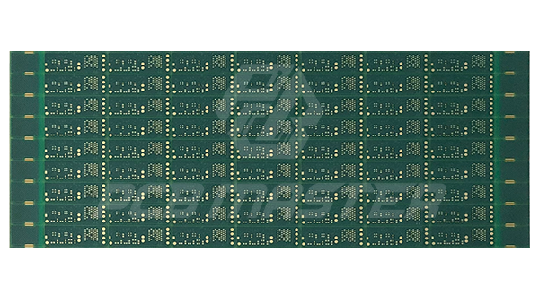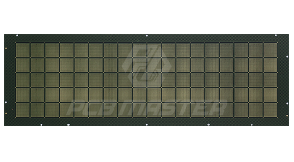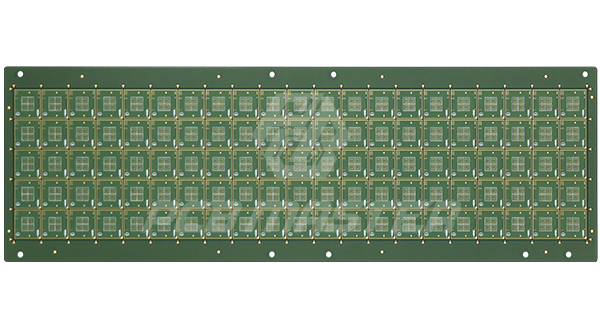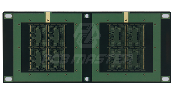








SiP IC Substrate
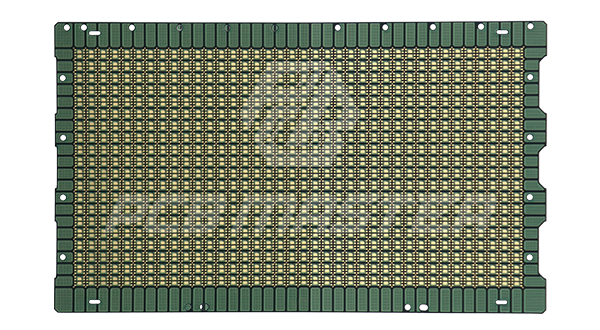
제품 사양
- Material BT
- Layer 2 layer
- Thickness 0.25mm
- Surface finish Electroless Nickel - Palladium - Gold: Nickel thickness 120 - 240U, Palladium thickness: 2U, Gold thickness: 3U
- Min Track/Spacing 0.05/0.03mm
- Special process The solder mask adopts the ink leveling process, and the ink flatness is within 8um. The Subtractive process flow is adopted.
- Min hole size 0.06mm
- Special technology Laser drilling with a hole diameter of 60um, small trace width and trace spacing. The dielectric thickness of the product is 0.05mm.