







PCB Staggered Edge Connector Contacts: Why Long and Short Gold Fingers Are Used
Modern electronic systems are expected to operate with near-zero tolerance for instability, especially when modules are inserted or removed during live operation. Yet behind many “plug-and-play” board-level failures lies a surprisingly subtle detail: how the edge connector contacts are physically staggered.
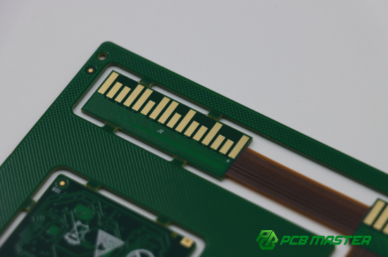
At first glance, gold fingers on a PCB edge connector may look uniform. However, in high-reliability designs such as PCIe cards, DIMM modules, and industrial hot-swap boards, the contact geometry is deliberately engineered with different lengths. This is not a cosmetic choice—it is a controlled electrical sequence embedded in hardware itself.
By shaping when ground, power, and signal paths make or break contact, designers can influence system behavior at the millisecond level. The result is a silent but critical mechanism that helps prevent electrostatic damage, avoids power sequencing faults, and stabilizes signal integrity during insertion and removal events.
Understanding this design approach reveals why edge connector geometry is treated as a functional part of system architecture rather than a simple mechanical interface.
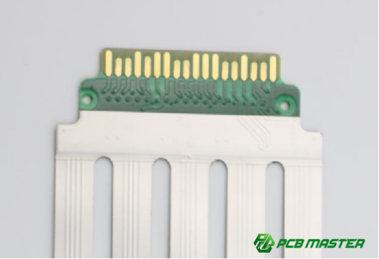
What is PCB Staggered Edge Connector Contacts and What Are Its Structural Characteristics?
PCB staggered edge connector contacts are PCB gold finger pads with intentionally different lengths that create a controlled insertion and removal sequence—typically grounding first, then power, and finally signal—to ensure safe electrical contact timing and system stability.
Basic Definition and Structural Form of Staggered Edge Contacts
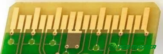
PCB long and short gold fingers are edge connector pads with intentionally different lengths to control the electrical contact sequence during insertion and removal.
Staggered edge connector contacts (also called long-short gold fingers or staggered PCB edge contacts ) are a structural design used on PCB edges where copper pads are intentionally made with different lengths instead of being uniform. This creates a controlled “contact timing difference” when a board is inserted into a connector.
The key difference between equal-length gold fingers vs staggered gold fingers is timing control:
- Equal-length fingers touch all contacts at the same moment.
- Staggered fingers create a controlled order of contact.
This design forms a hierarchical contact structure , typically:
- GND (Ground) first
- PWR (Power) second
- SIGNAL last
This sequence ensures the system always has a stable reference ground before power and data signals become active.
Simple example: Think of plugging in a device where the ground pin connects first, like setting a “foundation,” then power comes in like “fuel,” and finally signals act like “communication.” Without this order, the system can behave unpredictably.
Typical Arrangement of Staggered Edge Contacts in PCB Design
The typical arrangement is designed to ensure ground connects first, power stabilizes second, and signals activate last for safe system startup.
In most PCB edge connector designs (such as PCIe cards, DIMM modules, or industrial boards), the contact sequence follows a predictable safety order:
GND connects first (reference grounding stage)
Ground pads are designed longer so they touch the connector first during insertion. This ensures:
- A stable reference voltage is established immediately
- Electrostatic discharge (ESD) has a safe path to flow
- The system avoids floating voltage conditions
Example: In server hot-swap systems, ground contact first prevents random voltage spikes when a new board is inserted.
Power connects second (power stabilization stage)
Power pins are designed slightly shorter than ground but longer than signal pins. Their role is:
- Allow controlled power-up after ground is stable
- Reduce inrush current instability
- Enable pre-charge behavior in high-capacitance boards
Example: A board with large capacitors (e.g., 2200µF or more) benefits from this delay because it avoids sudden current surges.
Signal connects last (logic activation stage)
Signal pins are the shortest and connect last to ensure:
- The system is already powered and grounded before data transfer starts
- No false triggering occurs in chips or buses
- FPGA, CPU, or PHY interfaces initialize safely
Example: In PCIe systems, signal lines connecting last help prevent link training failures during insertion.
Physical Design Characteristics of PCB Edge Connectors
The physical design creates a controlled time delay in contact events using different finger lengths and insertion geometry.
Staggered gold fingers rely on physical length differences to generate a predictable contact sequence. Even a small difference in pad length (for example 0.5 mm to 1.5 mm) can create a measurable time delay during insertion.
This design creates a contact timing offset , meaning:
- Longer pads touch earlier
- Shorter pads touch later
- Each electrical group activates in a controlled sequence
Contact timing difference created by length variation
The main mechanism is simple: when the PCB is inserted into the connector slot, longer gold fingers physically reach the mating surface earlier than shorter ones. This converts mechanical motion into electrical timing control.
Example: If GND fingers are 1 mm longer than signal fingers, ground will always connect first even if the insertion speed varies.
Direction-dependent insertion and removal sequence control
Staggered edge connectors also control the break sequence when removing the board:
- Signal disconnects first (safe data shutdown)
- Power disconnects second (gradual power loss)
- Ground disconnects last (maintains reference until the end)
This prevents issues such as:
- Floating ground conditions
- Logic latch-up in ICs
- Unexpected voltage backflow
Real-world use case: In industrial control systems, improper disconnection can crash PLC modules. Staggered contacts ensure safe shutdown behavior even during accidental hot-unplug events.
Overall, PCB long-short gold finger design is not just a mechanical variation—it is a built-in timing control system that ensures electrical safety, signal integrity, and reliable hot-swapping behavior in high-performance electronic systems.
Why Must PCBs Use Long and Short Gold Fingers to Control Insertion and Removal Timing?
PCBs use long and short gold fingers to control insertion and removal timing so that ground, power, and signal connections are made and broken in a safe sequence, preventing electrical instability, signal errors, and hardware damage during hot-plug operations.
Risk Analysis of Simultaneous Contact During Insertion and Removal
If all gold fingers connect at the same time, the system can experience unstable power sequencing, logic errors, and even hardware damage.
In PCB edge connector design (long-short gold fingers) , simultaneous contact is dangerous because different electrical domains are not synchronized during insertion. Without controlled timing, the system powers up in an unpredictable order.
GND not established before power causes system instability
When ground (GND) is not connected first , but power is already applied , the circuit has no stable reference voltage. This can lead to:
- Floating voltage levels inside ICs
- Incorrect signal interpretation
- Unstable startup conditions
Example: In a PCIe hot-swap card, missing ground-first contact can cause the host system to detect an invalid device or fail enumeration.
Early signal activation causes logic errors or deadlock
If signal lines connect before power and ground are stable , digital chips may start reading random noise as valid data. This results in:
- Bus communication errors
- Firmware hang or deadlock
- False trigger of reset or control signals
Example: A DIMM memory module inserted without controlled timing may fail memory training due to premature signal activity.
Risk of chip mis-triggering and system crash
Uncontrolled insertion can cause partial power states , where some pins are active and others are not. This leads to:
- FPGA or CPU entering undefined states
- Latch-up conditions in CMOS circuits
- Full system crash or reboot
Real-world case: Industrial control boards without staggered contacts often fail during hot-plug events due to mixed voltage states across I/O pins.
Contact Timing Control Logic of Long and Short Gold Fingers
Long-short gold fingers create a fixed electrical sequence: ground first, power second, and signal last to ensure safe system startup.
The core idea of PCB staggered edge connector contacts is to convert physical length differences into a controlled electrical timing order.
Ground First principle and electrical meaning
Ground First means the system always establishes a stable reference voltage before anything else happens. This provides:
- A safe discharge path for static electricity (ESD protection)
- A stable voltage baseline for all circuits
- Reduced risk of floating signals
Simple explanation: Ground acts like “floor level” for electricity. Without it, everything else becomes unstable.
Power Second and stable power delivery mechanism
After ground is stable, power pins connect next to gradually energize the board. This allows:
- Controlled charging of large capacitors (inrush current reduction)
- Stable voltage ramp-up instead of sudden spikes
- Safer startup for power regulators and ICs
Example: In server power modules, staged power contact prevents sudden current surges that could damage connectors.
Signal Last logic safety strategy
Signals connect last because digital communication must only start when:
- Power is stable
- Ground reference is valid
- Internal chips are fully initialized
This prevents:
- False data transmission
- Communication bus conflicts
- FPGA/ASIC initialization errors
Example: In PCIe edge connector design, signal delay ensures proper link training only begins after stable power-up.
Importance of Reverse Disconnection Timing During Removal
Controlled disconnection prevents floating voltage states and protects circuits by ensuring signal, power, and ground break in a safe order.
When removing a PCB, the same timing logic works in reverse. This is critical for PCB hot swap safety and reliability .
Signal disconnects first to avoid floating interference
When signal lines break first , the system:
- Stops data communication immediately
- Prevents corrupted or partial data transmission
- Avoids ghost signals caused by unstable voltage
Example: In telecom boards, early signal break prevents packet corruption during unplugging.
Power disconnects gradually to reduce electrical shock
After signals stop, power is removed next , allowing:
- Controlled discharge of onboard capacitors
- Reduced voltage spike backflow into the system
- Lower stress on connectors and power regulators
Example: Industrial control systems rely on this step to prevent sudden resets or relay damage.
Ground disconnects last to maintain reference stability
Ground remains connected the longest to:
- Provide a safe discharge path until the very end
- Prevent floating ground conditions
- Stabilize final voltage equalization before full removal
Key idea: Ground is the “last safety anchor” before complete separation.
Overall, long-short gold finger design is essentially a hardware-based timing controller that ensures safe insertion and removal without software intervention, making it essential for PCIe, DIMM, and industrial hot-swap PCB systems.
What Is the Role of Long and Short Gold Fingers in Hot Swap (Hot-Plug) Systems?
Long and short gold fingers in hot swap (Hot-Plug) systems ensure a safe, fixed contact sequence—Ground first, Pre-charge second, Power third, and Signal last—so that boards can be inserted or removed while the system is running without causing electrical instability, bus errors, or system crashes.
Strict Contact Timing Requirements in Hot Swap Systems
Hot swap systems require precise contact sequencing to ensure boards can be inserted or removed while the system remains powered and stable.
In hot swap PCB design (Hot Plug PCB edge connector systems) , timing control is critical because the system is running while a new board is being inserted. Unlike normal electronics, there is no full shutdown, so even milliseconds of incorrect contact order can cause failure.
Application scenarios: PCIe, telecom, and industrial control boards
Long-short gold fingers are widely used in:
- PCIe hot-plug expansion cards in servers
- Telecom switching equipment requiring nonstop operation
- Industrial control backplanes with modular card slots
In these systems, any insertion must not interrupt the main system bus or power rail.
Example: A telecom base station must replace a faulty processing card without shutting down the network. Long-short edge connectors ensure safe live replacement.
Design constraint: insertion without system shutdown
Hot swap PCB design must support:
- Continuous power delivery during insertion/removal
- No reset of the backplane or host system
- Controlled electrical engagement of each pin group
This means PCB edge connector timing control (long-short gold fingers) is not optional—it is a core safety requirement.
Standard Contact Sequence Mechanism in Hot Swap Design
Hot swap systems use a fixed sequence—ground first, pre-charge second, power third, and signal last—to ensure safe electrical stabilization.
The standard hot swap contact sequence is designed to avoid sudden voltage spikes and communication errors during insertion.
Four-stage contact structure: GND → Pre-charge → Power → Signal
A typical hot swap PCB edge connector sequence follows:
- GND (Ground First): Establishes reference voltage and ESD protection
- Pre-charge: Slowly charges onboard capacitors through resistors
- Power: Applies stable operating voltage after pre-charge stabilization
- Signal: Activates data communication only after power is stable
This staged structure ensures that no part of the circuit receives unstable or unexpected voltage.
Example: In a server backplane, pre-charge pins prevent sudden 2200µF capacitor inrush currents that could damage connectors.
Key design goal: preventing Bus Error and Link Failure
Without controlled sequencing, systems may experience:
- Bus Error: Data lines activate before voltage stabilizes
- Link Failure: PCIe or communication links fail during training phase
- System hang: Devices enter undefined states during initialization
Long-short gold fingers ensure each stage activates only after the previous one is electrically stable.
System-Level Stability Improvement Mechanisms
Long-short gold fingers improve system reliability by ensuring proper initialization of chips and reducing system crashes during hot swap events.
In high-reliability PCB systems , contact timing directly affects how digital chips boot and communicate.
Preventing FPGA and ASIC initialization errors
FPGA and ASIC chips require:
- Stable power rails before configuration begins
- Valid clock and reset conditions
- Clean signal environment during startup
If signals arrive too early, the chip may:
- Enter incorrect boot states
- Fail configuration loading
- Lock into undefined logic conditions
Example: In industrial FPGA control boards, incorrect hot swap sequencing can corrupt bitstream loading, requiring a full system reset.
Reducing system reboot and bus hang probability
Proper hot swap sequencing helps:
- Avoid partial power states across the bus
- Prevent shared communication lines from locking
- Reduce full system reboot events
In PCIe and backplane systems , this ensures:
- Stable link training after insertion
- No frozen communication channels
- Continuous operation in redundant systems
Real-world benefit: In data centers, this design allows faulty cards to be replaced without affecting active workloads, improving uptime and system availability.
How Do Long and Short Gold Fingers Reduce ESD Shock and Inrush Current?
Long and short gold fingers reduce ESD shock and inrush current by enforcing a controlled contact sequence—ground first to safely discharge static electricity, followed by pre-charge and power to gradually charge capacitors, and signal last to prevent unstable electrical and data states during insertion.
Sources of ESD (Electrostatic Discharge) Risk
ESD risk in PCB edge connectors comes mainly from voltage differences during insertion and the sensitivity of IC input pins.
In PCB hot swap and edge connector systems (long-short gold fingers) , ESD happens when two conductive objects have different electrical potentials and suddenly touch. This creates a fast discharge path that can damage sensitive electronics.
Voltage difference during insertion creates discharge paths
When a PCB is inserted into a live system, the board and connector may have:
- Different static charge levels
- Different ground potential
- Unequal reference voltage
This mismatch causes a rapid electrostatic discharge (ESD event) through the first point of contact.
Example: If a board is charged to a few hundred volts static and suddenly touches a grounded connector pin, a tiny but powerful spark can occur, damaging micro-scale traces.
Sensitivity of chip I/O pins
Modern chips like FPGA, CPU, and high-speed PHY interfaces have:
- Very low voltage tolerance (often below 2–3V logic thresholds)
- Thin gate oxide structures
- Highly sensitive input buffers
Even a small ESD pulse can:
- Permanently damage I/O pins
- Cause latent failure (works now but fails later)
- Corrupt internal logic states
Real-world case: Industrial control boards often fail intermittently after ESD exposure due to hidden I/O degradation.
How Long and Short Gold Fingers Reduce ESD Impact
They reduce ESD damage by ensuring ground connects first and stabilizes voltage before power and signal contact occurs.
The PCB staggered edge connector design (long-short gold fingers) controls the order of contact so that unsafe voltage differences are eliminated early.
Priority grounding creates a safe discharge path
The longest pins are typically GND (Ground First) , which ensures:
- A stable reference voltage is established immediately
- Static electricity has a low-resistance path to discharge
- ESD energy is redirected safely away from sensitive circuits
Simple explanation: Ground acts like a “safety drain pipe” that removes static electricity before it reaches chips.
Reduced transient voltage difference (ΔV control)
By connecting ground first, the system reduces instantaneous voltage difference (ΔV) between board and connector.
This leads to:
- Lower peak ESD current
- Controlled equalization of electrical potential
- Reduced stress on IC input protection diodes
Example: In PCIe hot-plug systems, early ground connection prevents signal pins from seeing sudden voltage spikes during insertion.
Inrush Current Control Methods in PCB Edge Design
Inrush current is controlled by pre-charging capacitors and gradually stabilizing power instead of applying full voltage instantly.
When a PCB with large capacitors is connected to a power source, it behaves like a “short circuit for a moment,” causing a sudden current spike known as Inrush Current .
Pre-charge structure using resistors
A key method in hot swap PCB design is the use of a pre-charge contact (Pre-charge pin) :
- Connects before full power pins
- Uses a resistor to limit current
- Slowly raises voltage on board capacitors
This prevents:
- Connector arcing
- Power rail collapse
- System reset due to voltage drop
Example: Server backplanes often include pre-charge pins to safely energize large power modules.
Slow charging of large capacitors (1000µF+)
Boards often contain large capacitors (e.g., 1000µF, 2200µF, or higher). Without control:
- They draw extremely high initial current
- This can stress connectors and power supply units
With staged charging:
- Capacitors charge gradually
- Voltage rises smoothly instead of instantly
- Power stability improves during insertion
Simple analogy: It is like filling a large water tank slowly through a small pipe instead of dumping all water at once.
Reducing contact burn and voltage drop risk
Controlled inrush current helps:
- Prevent burning or pitting of gold finger contacts
- Reduce voltage dips on the main power rail
- Improve long-term connector lifespan
Real-world benefit: In industrial hot-swap systems, this design significantly increases connector durability and reduces maintenance failures caused by contact erosion.
Overall, long-short gold finger design improves both ESD protection and inrush current control by enforcing a physical contact sequence that ensures safe electrical equalization before full system power and signal activation.
Practical Applications of PCB Long and Short Gold Fingers in PCIe, DIMM, and Industrial Boards
PCB long and short gold fingers are used in PCIe, DIMM, and industrial boards to control insertion timing so that ground, power, and signal connect in a safe sequence, ensuring stable system detection, reliable initialization, and support for hot-swappable high-reliability operation.
PCIe Expansion Card Timing Design
In PCIe systems, long and short gold fingers ensure a safe contact sequence so that ground and key control signals connect before power and high-speed data lines.
In PCIe edge connector design (PCIe hot-plug PCB long-short gold fingers) , timing control is essential because the system may detect and initialize a card immediately upon insertion.
PRSNT# and GND priority contact logic
In PCIe expansion cards:
- GND pins are designed longer to establish a stable reference first
- PRSNT# (presence detect pin) often connects early to inform the system that a card is being inserted
This ensures:
- The motherboard detects the card safely
- Ground reference is stable before any power or signal activity begins
- No false detection or random bus triggering occurs
Example: In server PCIe hot-swap slots, PRSNT# early contact prevents the system from powering incorrect slot configurations.
Compliance with PCI Express Base Specification
The PCI Express Base Specification requires:
- Controlled power sequencing during insertion
- Defined contact order for hot-plug capable slots
- Stable ground before signal activation
Long-short gold finger design helps meet these requirements by:
- Ensuring deterministic insertion timing
- Reducing PCIe link training failures
- Preventing undefined electrical states during initialization
Real-world case: High-performance servers rely on this design to avoid PCIe link drops when replacing GPUs or NVMe expansion cards during operation.
DIMM Memory Module Contact Control
DIMM modules use staggered gold finger contact to ensure stable power and signal sequencing, preventing memory initialization failures during insertion.
In DIMM memory connector design (DDR memory slot edge contact control) , timing is critical because memory initialization is extremely sensitive to voltage stability.
Stability requirement for power and signal separation
DIMM modules require:
- Power pins to connect in a controlled order
- Signal lines to activate only after stable voltage is present
Long-short gold fingers ensure:
- VDD/VSS (power and ground) stabilize first
- Address and data signals connect later
This avoids:
- Voltage glitches during boot
- Unstable DRAM refresh cycles
- Incorrect memory training behavior
Example: In DDR4/DDR5 systems, improper sequencing can cause BIOS memory detection failure.
Preventing memory initialization failure
If DIMM contacts connect simultaneously:
- Memory controller may read unstable signals
- DRAM training sequence may fail
- System may not boot or detect RAM capacity correctly
With staggered contacts:
- Stable power is guaranteed before logic activation
- Reset and clock signals are properly synchronized
- Memory initialization becomes reliable
Real-world example: Server-grade ECC memory systems depend on precise contact timing to avoid boot-time memory errors in multi-DIMM configurations.
Industrial and Military-Grade Board Applications
Industrial and military systems use long-short gold fingers to achieve high-reliability hot swapping, vibration resistance, and standardized backplane connectivity.
In industrial PCB edge connector systems (VPX, CompactPCI, ATCA long-short gold finger design) , reliability is more important than speed or cost.
VPX, CompactPCI, and ATCA system standards
These high-reliability platforms require:
- Defined insertion and extraction sequences
- Hot-swappable module support
- Backplane-based modular architecture
Long-short gold fingers help:
- Ensure safe live insertion in VPX defense systems
- Maintain system uptime in telecom ATCA racks
- Support modular upgrades in CompactPCI industrial controllers
Example: In ATCA telecom systems, a line card can be replaced without shutting down the entire switching system.
High reliability insertion and vibration resistance requirements
Industrial and military environments require connectors that:
- Resist mechanical vibration and shock
- Maintain stable contact under repeated insertion cycles
- Prevent accidental signal corruption during movement
Long-short gold finger design improves:
- Mechanical contact reliability
- Electrical stability under vibration
- Reduced risk of intermittent connection failure
Real-world case: In aerospace or rail control systems, staggered contacts ensure that vibration during operation does not cause transient signal loss or system resets.
Overall, PCB long and short gold fingers in PCIe, DIMM, and industrial boards are a core design mechanism that ensures safe power sequencing, stable initialization, and high-reliability hot-swapping across modern electronic systems.

Key Design Parameters of PCB Long and Short Gold Fingers
The key design parameters of PCB long and short gold fingers include controlled length differences (typically 0.5–5 mm depending on application), hard gold plating thickness (15–100 μin) for durability, optimized bevel angles (20°–45°) for smooth insertion, and strict differential pair constraints to maintain signal integrity while ensuring safe and reliable contact sequencing.
Design Range of Length Difference (Engineering Reference Values)
The length difference of PCB long and short gold fingers is typically chosen based on application reliability level, ranging from 0.5 mm in industrial boards to up to 5 mm in military systems.
In PCB staggered edge connector design (long-short gold fingers timing control) , the length difference directly determines the contact delay between ground, power, and signal pins. A larger difference creates a longer and more stable sequencing window.
Industrial boards: 0.5–1.0 mm
Used in standard industrial control systems:
- Moderate insertion speed
- Limited hot-swap requirement
- Balanced cost and reliability
Example: PLC control modules use ~0.8 mm offset to ensure basic safe sequencing without excessive connector wear.
PCIe systems: 0.5–1.5 mm
Used in servers and high-speed computing:
·Requires stable PRSNT# and GND timing
·Must follow PCIe hot-plug behavior
Example: GPU server cards use ~1.0 mm offset to ensure correct link training during insertion.
Hot-swap systems: 1–3 mm
Used in live replacement environments:
·Higher tolerance for insertion speed variation
·Stronger protection against inrush current and ESD
Example: Telecom hot-swap line cards use up to 2 mm offset to guarantee safe power sequencing.
Military-grade high reliability: 2–5 mm
Used in extreme environments:
·Shock, vibration, and unstable insertion conditions
·Maximum timing safety margin required
Example: Aerospace VPX modules use larger offsets to ensure safe operation under vibration and field replacement.
Surface Treatment and Mechanical Structure Design
Hard gold plating thickness and insertion durability directly affect contact reliability and lifespan of PCB edge connectors.
In PCB gold finger design (hard gold PCB edge connector reliability engineering) , surface treatment determines how well contacts survive repeated insertion cycles.
Hard Gold plating thickness (15–100 μin)
Hard gold (electroplated nickel-gold) is used because:
·It resists wear from repeated insertion
·It maintains stable conductivity over time
Common ranges:
·15–30 μin: low-cycle consumer/industrial use
·30–50 μin: standard server and telecom use
·50–100 μin: high-cycle military or mission-critical systems
Example: A telecom hot-swap backplane may use 30 μin hard gold for balanced cost and durability.
Relationship between insertion cycles and reliability
More insertion cycles require:
·Thicker gold plating
·Stronger nickel underlayer
·Lower contact resistance stability
Simple explanation: The more you plug/unplug a card, the thicker and stronger the gold layer must be to avoid wear-out and signal degradation.
Bevel (Chamfer) Design and Insertion Optimization
Bevel design reduces insertion force and wear by guiding the PCB edge smoothly into the connector.
In PCB edge connector mechanical design (gold finger bevel optimization) , chamfered edges help protect both connector and PCB during repeated insertion.
20° / 30° / 45° bevel angles
Common bevel angles serve different purposes:
· 20°: Smoothest insertion, highest precision systems
· 30°: Balanced industrial standard
· 45°: Cost-effective, easier manufacturing
Example: High-density PCIe cards often use 30° bevel for smooth server insertion.
Reducing wear and insertion force
Bevel design helps:
·Reduce mechanical scraping of gold fingers
·Lower insertion force (easier hot-swap operation)
·Prevent connector deformation over time
Simple analogy: It is like sliding a knife into a slot with a rounded tip instead of a flat edge.
Differential Pair Design Constraints
Differential pairs must remain length-matched and impedance-controlled, even when using staggered contact timing at group level.
In high-speed PCB design (PCIe/DDR differential pair routing with staggered edge connectors) , signal integrity is critical.
Differential pairs must remain length-matched for impedance consistency
Rules include:
·Both traces in a differential pair must be equal length
·Maintain controlled impedance (e.g., 85Ω or 100Ω)
·Avoid skew between + and – signals
Example: PCIe TX/RX lanes must remain tightly matched to avoid data corruption at multi-gigabit speeds.
Only group-level timing offset is allowed
Long-short gold fingers can only shift:
·Entire functional groups (e.g., power vs signal groups)
They must NOT:
·Break differential pair symmetry
·Introduce internal pair skew
Simple explanation: You can delay when a group connects, but you cannot “separate twins” inside a high-speed signal pair.
Overall, PCB long and short gold finger design parameters balance electrical safety, mechanical durability, and high-speed signal integrity, making them essential for reliable PCIe, industrial, and military-grade connector systems.
Conclusion
Long and short gold fingers are far more than a mechanical variation on a PCB edge—they represent a carefully engineered electrical sequencing method that directly impacts system safety, signal integrity, and hot-swap reliability. By controlling the order of ground, power, and signal contact, this design helps prevent ESD damage, reduces inrush current stress, and ensures stable initialization across demanding applications such as PCIe, DIMM, and industrial backplane systems.
As electronic systems continue to evolve toward higher speed, higher density, and uninterrupted operation, the importance of precise connector design only becomes more critical. Even small details such as contact length differences, plating thickness, and bevel geometry can determine whether a system operates smoothly or fails under real-world conditions.
Against this backdrop of increasingly strict reliability requirements, choosing a manufacturing partner with deep engineering experience becomes essential. This is where PCBMASTER , a seasoned PCB and PCBA supplier , comes into focus. With strong expertise in high-reliability PCB fabrication and assembly, PCBMASTER supports complex designs that demand tight control over electrical performance and mechanical precision, helping engineers translate advanced connector concepts into dependable, production-ready hardware.
FAQs
Are long and short gold fingers required for all PCBs?
No, long and short gold fingers are only necessary for PCBs that require hot-swapping or high-reliability operation.
Their use is mainly driven by system needs such as live insertion, power stability, and ESD protection. For standard consumer electronics that are powered on/off normally, equal-length gold fingers are usually sufficient and more cost-effective.
How is the optimal length difference of gold fingers determined?
The optimal length difference is determined by insertion speed, capacitive load, and system design standards.
Faster insertion speeds or higher-capacitance boards require larger length differences to ensure stable sequencing. Engineers also follow platform specifications (such as PCIe or industrial backplane standards) to define safe timing margins for ground, power, and signal contact.
Can only power be staggered while keeping signal short?
Yes, but the full contact sequence logic must still follow Ground-first principles.
In some designs, power pins are extended while signal pins are shorter to control power-up timing. However, ground must always connect first to establish a stable reference; otherwise, the system may experience ESD or unstable voltage behavior.
Does long-short gold finger design affect signal integrity?
No, it does not affect differential pair signal integrity if designed correctly.
Long-short gold fingers only control the timing of contact , not the electrical structure of high-speed routing. Differential pairs remain length-matched on the PCB itself, so impedance and skew are not impacted, provided the design does not break pair symmetry.
Why must PCIe use staggered (graded) gold finger design?
PCIe requires staggered gold fingers to ensure hot-plug stability and specification-compliant power sequencing.
The PCIe standard defines strict requirements for insertion behavior, including controlled ground, power, and signal activation order. Staggered contacts help prevent link training failures, bus errors, and system instability during live insertion or removal of expansion cards.
About the Author

Carol Luo
PCB Design EngineerI'm Carol, a PCB Engineer at PCBMASTER with experience in PCB design and manufacturing engineering since 2018. I focus on translating engineering requirements into reliable PCB solutions, with expertise in stack-up design, material selection, and design-for-manufacturing (DFM). I share practical engineering insights from real-world PCB design and production experience.
Visit Carol Luo's Profile