







Capacitor Symbol: Complete Guide to Capacitor Schematic Symbols and Their Meanings
A capacitor symbol is a standardized graphical representation used in circuit schematics to identify a capacitor and indicate its electrical characteristics or polarity. The most common symbol consists of two parallel plates, while polarized capacitors, variable capacitors, and other specialized types use modified symbols. Understanding these symbols helps engineers read schematics, select appropriate components, and translate circuit designs into PCB layouts accurately.
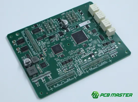
What Is a Capacitor Symbol?
A capacitor symbol is the graphical representation of a capacitor in an electrical schematic. It communicates that a circuit contains a component designed to store and release electrical energy in an electric field .
The basic capacitor symbol consists of two conductive plates separated by a gap , representing the two electrodes and dielectric material between them.
A typical non-polarized capacitor is represented as:
───| |───
The exact graphical style can vary depending on the schematic standard, CAD software, and region, but the underlying meaning remains the same.
For PCB and PCBA engineers, recognizing capacitor symbols is important because the schematic is the starting point for component selection, PCB layout, BOM generation, and assembly.
What Does the Basic Capacitor Symbol Mean?
The standard capacitor symbol generally contains two parallel lines or plates.
| Symbol Element | Meaning |
|---|---|
| Two parallel plates | Capacitor electrodes |
| Gap between plates | Dielectric material |
| C | Common reference designator for a capacitor |
| Connection lines | Electrical connections to the circuit |
The reference designator C is commonly used to identify capacitors in schematics.
For example:
C1
───| |───
Here, C1 identifies the first capacitor in the circuit.
Other capacitors might be labeled C2, C3, C4, and so on.
The schematic symbol itself does not normally communicate the capacitance value. The value is typically specified separately, such as:
- 10 pF
- 100 pF
- 1 nF
- 100 nF
- 1 µF
- 10 µF
- 100 µF
Common Types of Capacitor Symbols
Not every capacitor uses the same schematic symbol. The symbol can change according to whether the component is polarized, adjustable, or designed for a particular electrical application.
Non-Polarized Capacitor Symbol
A standard non-polarized capacitor is represented by two parallel plates:
───| |───
This symbol is commonly used for ceramic capacitors, film capacitors, and other capacitors that do not require a defined positive and negative orientation.
Because the component is non-polarized, it can generally be installed in either orientation.
Common applications include:
- Decoupling
- High-frequency filtering
- Signal coupling
- Noise suppression
- Timing circuits
- Resonant circuits
Polarized Capacitor Symbol
Polarized capacitors require a specific electrical orientation.
A polarized capacitor symbol typically includes a positive (+) indication or another graphical marking that identifies the positive terminal.
───| |───
+
The exact representation depends on the schematic convention.
Common polarized capacitors include:
- Aluminum electrolytic capacitors
- Tantalum capacitors
- Polymer capacitors
Polarity is particularly important during PCB assembly. Installing a polarized capacitor incorrectly can cause electrical failure and, in some cases, physical damage to the component.
Variable Capacitor Symbol
A variable capacitor allows its capacitance to be adjusted.
Its symbol resembles a conventional capacitor with a diagonal arrow through or across the capacitor plates.
───| |───
↗
Variable capacitors are used where capacitance needs to be tuned, such as:
- RF circuits
- Oscillators
- Tuning circuits
- Antenna matching networks
- Frequency adjustment circuits
Trimmer Capacitor Symbol
A trimmer capacitor is a small adjustable capacitor designed primarily for calibration rather than frequent adjustment.
Its schematic symbol is similar to that of a variable capacitor, although the exact representation varies according to the drafting standard.
Trimmer capacitors are often found in RF and precision electronic circuits where circuit parameters must be calibrated after manufacturing.
Capacitor Symbols vs. Real Capacitor Packages
One important concept for PCB designers is that the schematic symbol does not represent the physical shape of the capacitor .
For example, the same electrical capacitor symbol could correspond to several physical packages:
| Schematic | Possible Physical Component |
|---|---|
| Non-polarized capacitor | 0201, 0402, 0603, 0805 MLCC |
| Non-polarized capacitor | Through-hole film capacitor |
| Polarized capacitor | SMD electrolytic |
| Polarized capacitor | Radial electrolytic |
| Polarized capacitor | Tantalum capacitor |
| Variable capacitor | Adjustable through-hole or SMD component |
The schematic represents the electrical function , while the PCB footprint represents the physical implementation .
This distinction becomes particularly important when converting an electrical schematic into a manufacturable PCB design.
How Capacitor Symbols Appear in PCB Schematics
In an electronic design workflow, capacitors are normally assigned reference designators beginning with C .
For example:
C1 = 100 nF
C2 = 10 µF
C3 = 1 µF
A schematic may therefore contain dozens or even hundreds of capacitor symbols.
A simplified power circuit could look like:
VCC ──────┬──────── IC
│
C1
│
GND
Here, C1 may serve as a decoupling capacitor between the power rail and ground.
A more complex circuit could contain:
- Input filtering capacitors
- Output filtering capacitors
- IC decoupling capacitors
- Bulk capacitors
- AC coupling capacitors
- Snubber capacitors
- Timing capacitors
- EMI suppression capacitors
Although these components share the same basic function, their capacitance, voltage rating, dielectric, package, ESR, ESL, and placement requirements can be significantly different.
Why Capacitor Symbols Matter in PCB Design
Understanding capacitor symbols is more than a schematic-reading skill.
The capacitor's electrical role directly affects PCB layout.
Decoupling Capacitors
Decoupling capacitors are commonly placed close to IC power pins.
The PCB designer needs to minimize the impedance between:
IC power pin → capacitor → ground
A suitable capacitor symbol in the schematic establishes the intended electrical connection, while PCB placement and routing determine whether the physical implementation achieves the desired electrical performance.
Power Supply Filtering
Larger capacitors may be used on power input and output rails to reduce voltage fluctuations and filter low-frequency disturbances.
The schematic helps identify these components and their relationship with the power supply network.
High-Speed Circuits
High-speed digital and RF designs require greater attention to parasitic effects.
The capacitor's:
- ESR
- ESL
- Self-resonant frequency
- Package size
- Mounting location
- Via configuration
can influence actual circuit performance.
Therefore, a simple capacitor symbol in a schematic can correspond to a much more complex PCB design decision.
Capacitor Symbol and Polarity: A Critical PCB Consideration
One of the most important differences between capacitor symbols is polarity .
A non-polarized capacitor can generally be connected in either direction.
A polarized capacitor cannot.
For example, an electrolytic capacitor may have:
+ ───| |─── -
The positive terminal must be connected to the appropriate positive potential.
During PCBA production, polarity information must be correctly transferred across:
Schematic → PCB layout → BOM → Pick-and-place data → Assembly → Inspection
An error at any stage can result in a defective assembly.
This is one reason why schematic review and engineering file checking are important before PCB fabrication and assembly.
Common Capacitor Symbol Mistakes
Mistake 1: Assuming All Capacitors Are Polarized
Not all capacitors have polarity.
Ceramic and film capacitors are typically non-polarized, while many electrolytic and tantalum capacitors are polarized.
Mistake 2: Ignoring the Capacitor's Actual Specification
A capacitor symbol alone does not tell you whether a component is suitable for an application.
Engineers should also consider:
- Capacitance
- Voltage rating
- Tolerance
- Dielectric
- Temperature characteristics
- ESR
- ESL
- Package
- DC bias characteristics for MLCCs
Mistake 3: Treating the Schematic Symbol as the PCB Footprint
The symbol describes the electrical component.
The footprint defines how the component is physically mounted on the PCB.
These are separate design objects and must be correctly associated.
Mistake 4: Failing to Check Polarity Before Assembly
For polarized capacitors, polarity must be consistent between the schematic, PCB footprint, silkscreen, BOM, and assembly data.
Capacitor Symbol vs. Resistor Symbol
Capacitors and resistors are two of the most frequently encountered passive components in PCB schematics.
| Feature | Capacitor | Resistor |
|---|---|---|
| Common reference | C | R |
| Primary function | Stores electrical energy | Limits/opposes current |
| Basic symbol | Two plates | Zigzag or rectangular element |
| Polarity | Depends on type | Generally non-polarized |
| Common applications | Filtering, coupling, decoupling | Current limiting, voltage division, biasing |
| Typical PCB packages | 0201–1210, electrolytic, film | 0201–2512, through-hole |
Recognizing these symbols allows engineers to understand a schematic much faster.
How to Read a Capacitor Symbol in a Schematic
A practical approach is to evaluate five pieces of information:
- Reference designator— such as C1 or C25.
- Symbol type— determine whether the capacitor is polarized, variable, or standard.
- Electrical value— identify the capacitance and voltage requirements.
- Circuit location— determine whether it is used for filtering, coupling, timing, decoupling, or another purpose.
- Physical implementation— verify the footprint, package, orientation, and PCB placement.
This approach helps connect the schematic-level design intent with PCB manufacturing requirements.
How PCBMASTER Approaches Capacitor-Related PCB Manufacturing
As a PCB and PCBA manufacturer, PCBMASTER supports projects in which component selection, PCB fabrication, assembly, and engineering review must remain consistent throughout the production process.
Its manufacturing capabilities cover standard PCBs as well as HDI , high-frequency , FPC , rigid-flex , and metal-core PCBs , allowing capacitor placement and interconnection requirements to be considered within different PCB technologies.
PCBMASTER also provides free engineering file checking , allowing engineers to review manufacturability and identify potential design issues before production.
For PCBA projects, this connection between schematic information, component data, PCB fabrication, and assembly is particularly important because capacitor polarity, footprint selection, placement, and soldering requirements can directly affect production quality.
The company operates an 80,000 m² factory and provides PCB and PCBA services from manufacturing and assembly to component sourcing and engineering support. Its quality system includes ISO 9001, IATF 16949, UL, and RoHS certifications.
Practical Checklist for Working With Capacitor Symbols
Before releasing a PCB project for manufacturing, engineers can check:
- Is the capacitor symbol correct?
- Is the capacitor polarized or non-polarized?
- Does the capacitance value meet the circuit requirement?
- Is the voltage rating sufficient?
- Is the correct footprint assigned?
- Does the PCB footprint indicate polarity correctly?
- Is the component package suitable for assembly?
- Are decoupling capacitors positioned appropriately?
- Does the BOM match the schematic and PCB?
- Have the manufacturing files been reviewed?
For high-density PCB designs, additional considerations may include capacitor package size, placement density, thermal constraints, power integrity, and accessibility for automated SMT assembly.
Conclusion
The capacitor symbol is a fundamental element of electronic schematics, but understanding it requires more than recognizing two parallel plates. Engineers need to distinguish between non-polarized, polarized, variable, and specialized capacitor symbols , then connect the schematic representation with the component's electrical specifications and physical PCB implementation.
For PCB design and manufacturing, the critical workflow is:
Capacitor Symbol → Component Specification → Footprint → PCB Layout → BOM → PCBA → Testing
Correct interpretation at the schematic stage helps prevent component polarity errors, footprint mismatches, and manufacturing problems later in the process. For complex PCB and PCBA projects, engineering review and manufacturability verification provide an additional layer of control before production.
Tags
#CapacitorSymbol #Capacitor #PCB #PCBA #PCBDesign #CircuitDesign #Electronics #SMT #PCBManufacturing #ElectronicComponents #EngineeringInsights
About the Author

Carol Luo
PCB Design EngineerI'm Carol, a PCB Engineer at PCBMASTER with experience in PCB design and manufacturing engineering since 2018. I focus on translating engineering requirements into reliable PCB solutions, with expertise in stack-up design, material selection, and design-for-manufacturing (DFM). I share practical engineering insights from real-world PCB design and production experience.
Visit Carol Luo's Profile