








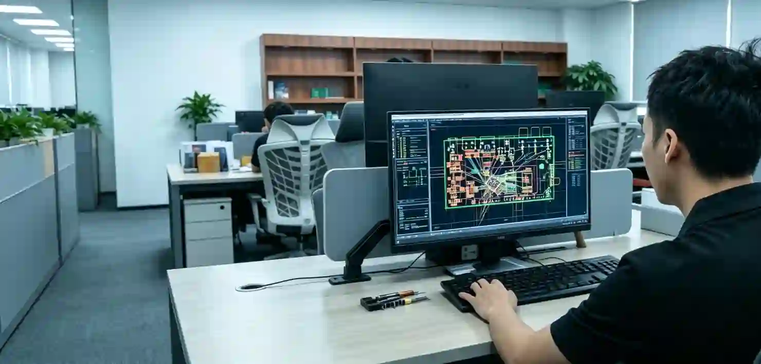
Professional PCB Design Services for Complex Electronics
From schematic to production-ready PCB, PCBMASTER provides you with engineering expertise to optimize performance, manufacturability, cost, and reliability—with a direct path from design to production.
- ✓ Turn Your Schematic Into a Production-Ready PCB
- ✓ Optimize Layout for Performance, Reliability & Cost
- ✓ Solve High-Speed, High-Frequency & Complex PCB Challenges
- ✓ Design, Prototype, Manufacture & Assemble With One Partner
なぜPCBMASTERなのか
Why Choose PCBMASTER for PCB Design?
PCBMASTER provides PCB Design services that go beyond layout. We help you address design, performance, manufacturability, and production challenges—from engineering review to PCB manufacturing and PCBA.
Design for Manufacturing
Our PCB Design process incorporates DFM requirements from the beginning, helping identify fabrication and assembly issues early and reduce costly redesigns before production.
Complex PCB Design Capability
Our engineering team supports HDI, high-speed, high-frequency, multilayer, flexible, and rigid-flex PCB designs while balancing electrical, mechanical, and manufacturing requirements.
Engineering-Driven Design Optimization
Experienced PCB engineers support schematic review, component placement, stack-up, routing, and impedance control to help optimize signal integrity, power distribution, and thermal performance.
Reduced Design-to-Production Risk
We review your PCB Design against manufacturing requirements before fabrication, helping identify DFM and assembly issues early and reduce unnecessary design iterations.
Design-to-PCBA Integration
With PCBMASTER, your project can move directly from PCB Design to PCB fabrication, component sourcing, SMT, THT, PCBA testing, and production through one integrated partner.
What Is PCB Design?
You may already have a schematic, product concept, or partially completed design—but turning it into a reliable, manufacturable PCB requires much more than routing traces. PCB Design connects your electrical requirements with the physical board, component selection, manufacturing constraints, and product performance.
A complete PCB Design process can include schematic review, component placement, PCB layout, layer stack-up, routing, power distribution, signal integrity, thermal management, DFM, DFT, and manufacturing preparation. Each step helps ensure that your PCB can meet its electrical and mechanical requirements while remaining practical to fabricate, assemble, test, and scale.
Ready to Turn Your PCB Design Into a Production-Ready Board?
From Your Schematic to a Production-Ready PCB
A reliable PCB Design requires more than completing the layout. PCBMASTER takes you through a structured engineering process—from reviewing your requirements and schematic to validating the design and preparing it for PCB manufacturing and PCBA.
Design Requirement Review
We review your application, technical specifications, components, interfaces, board constraints, and manufacturing requirements to establish the right design approach.
Schematic & BOM Review
Your schematic and BOM are checked for connectivity, component availability, footprints, and potential design risks before layout begins.
Layer Stack-Up Design
We define the layer count, dielectric structure, copper thickness, material selection, and impedance requirements according to your electrical and mechanical needs.
部品実装
Components are positioned to support signal integrity, thermal performance, EMI control, accessibility, and manufacturability.
PCB Routing
We route high-speed, power, analog, digital, and sensitive signals according to your design requirements, with attention to critical paths and return paths.
SI / PI & Design Validation
Critical interfaces are reviewed for signal integrity, power integrity, impedance, return paths, and other electrical performance requirements.
DFM / DFT Review
The design is reviewed for fabrication, assembly, inspection, and testing requirements to help reduce manufacturing issues and unnecessary redesigns.
Manufacturing Files
We prepare production documentation including Gerber or ODB++, drill files, fabrication drawings, BOM, and other required manufacturing data.
Prototype & Validation
Your PCB prototype can be fabricated and validated before production scaling, allowing potential design or manufacturing issues to be identified early.
Production
After validation, your design can move directly into PCB fabrication, component sourcing, PCBA assembly, testing, and production through PCBMASTER.
Explore PCB Design Services from PCBMASTER
PCBMASTER provides a wide range of PCB Design services to support different product structures, electrical requirements, performance demands, and mechanical constraints.
Standard PCB Design
For conventional electronic products with straightforward circuit requirements, Standard PCB Design provides a practical and cost-effective layout without unnecessary structural complexity. It is suitable when your design does not require HDI, flexible structures, high-speed routing, or specialized materials.
Multilayer PCB Design
When a single- or double-sided board no longer provides enough routing space, Multilayer PCB Design gives you additional layers for complex interconnections, power distribution, and signal routing. It is a good choice for increasingly dense electronic systems that need more functionality within a limited board area.
HDI PCB Design
If your product needs to become smaller while accommodating more components and connections, HDI PCB Design helps increase wiring density within a compact footprint. Microvias, blind/buried vias, and fine-pitch routing make HDI suitable for space-constrained and highly integrated electronics.
Flexible PCB / FPC Design
When your circuit needs to bend, fold, or fit into narrow and irregular spaces, Flexible PCB / FPC Design provides the mechanical flexibility that rigid boards cannot. It is ideal for lightweight and space-constrained products where conventional PCB structures limit product design.
Rigid-Flex PCB Design
When your product requires both structural rigidity and flexible connections, Rigid-Flex PCB Design combines rigid and flexible sections within one board structure. This can help reduce connectors, cables, assembly space, and mechanical integration challenges.
High-Speed PCB Design
When high-speed interfaces become critical to system performance, conventional routing is often not enough. High-Speed PCB Design addresses impedance control, signal integrity, return paths, crosstalk, and stack-up requirements to support reliable transmission across demanding interfaces.
High-Frequency PCB Design
For RF and high-frequency circuits, small changes in materials, geometry, grounding, and impedance can significantly affect performance. High-Frequency PCB Design uses appropriate materials, stack-ups, controlled-impedance structures, and grounding strategies for demanding high-frequency applications.
High-Power PCB Design
When your PCB must carry high current or handle significant power, the layout needs to account for current capacity, copper distribution, voltage drop, heat generation, and component temperature. High-Power PCB Design helps create a safer and more reliable power delivery structure.
Metal Core PCB Design
When heat dissipation becomes a major limitation for your electronic design, Metal Core PCB Design provides an enhanced thermal path compared with conventional PCB structures. It is particularly suitable for power components, LED systems, and other applications where efficient heat transfer is essential.
Ceramic PCB Design
For applications exposed to demanding thermal, electrical, or high-frequency conditions, Ceramic PCB Design offers properties beyond conventional organic substrates. It is suitable when high thermal conductivity, dimensional stability, electrical insulation, or high-frequency performance is a priority.
Ultra-Long PCB Design
When your product requires an unusually long circuit board, standard PCB design approaches may not adequately address the resulting electrical, mechanical, and manufacturing challenges. Ultra-Long PCB Design helps maintain consistent performance and structural feasibility across extended board dimensions.
IC Substrate Design
When semiconductor packaging requires extremely fine-pitch interconnections and very high wiring density, IC Substrate Design provides the specialized structure needed between the IC and the next level of interconnection. It is suited to advanced semiconductor packaging and compact high-density electronic systems.
PCB Design Capability at a Glance
PCBMASTER provides PCB Design services for standard and advanced electronic products, with engineering capabilities covering complex multilayer, HDI, high-speed, high-frequency, high-power, flexible, and rigid-flex designs. Your design can also move directly into PCB manufacturing and PCBA through the same integrated workflow.
| 能力 | PCBMASTER Details |
|---|---|
| PCB Design Types | Rigid PCB, Flexible PCB, Rigid-Flex PCB, High-Speed, High-Frequency, High-Power, HDI Any-Layer |
| Layer & Stack-Up Design | Supports 20+ layer high-speed stack-up design and complex multilayer PCB structures |
| HDI Design | HDI Any-Layer design with microvias, blind/buried vias, and high-density interconnections |
| High-Speed Design | High-speed interface design with controlled impedance and ±5% impedance tolerance |
| High-Frequency Design | RF and high-frequency PCB Design using specialized materials such as Rogers and Teflon |
| High-Power Design | Supports heavy-copper design with up to 10 oz copper foil for demanding power applications |
| Flexible & Rigid-Flex Design | Flexible PCB and rigid-flex layouts for compact, bendable, and space-constrained products |
| Ultra-Thin Design | PCB designs supporting board thickness down to 0.2 mm for space-constrained applications |
| DFM / Manufacturing Support | Design considerations aligned with PCB fabrication, assembly, inspection, and production requirements |
| PCB製造 | Direct transition from design to prototype, small-batch, and mass production, with PCB production up to 64 layers |
| PCBアセンブリ | SMT, THT, and mixed assembly, including fine-pitch and 01005 components |
| 部品調達 | Component sourcing available for PCBA projects, with turnkey, kitted, and consigned supply options |
| 材料 | FR-4, high-speed/high-frequency laminates, flexible materials, metal-core, ceramic, PTFE, IC substrate, and other specialty materials |
| Quality & Standards | IATF 16949, ISO 9001, UL Certification, and RoHS; IPC Class 3 design support |
From Your Design to Your Finished PCB
You bring the product concept. PCBMASTER helps turn it into a manufacturable PCB and scalable PCBA—from engineering review and prototype validation to production.
Start Your PCB Design
Find the Right PCB Design Solution for Your Project
Whether you are starting from a schematic, improving an existing PCB, solving a technical challenge, or preparing for production, PCBMASTER provides PCB Design support to help you move your project forward with greater confidence.
Starting from a Schematic?
Turn your circuit concept into a complete, production-ready PCB layout. Our engineers can help with component placement, routing, layer stack-up, power distribution, and manufacturing documentation, giving you a clear path from schematic to physical board.
Have an Existing PCB Design?
Improve an existing design before it becomes a production problem. We can review your PCB layout and help identify opportunities to improve performance, manufacturability, reliability, board cost, or component placement before you move into fabrication.
Need a Smaller PCB?
Fit more functionality into a smaller board without compromising manufacturability. Our design approach can optimize component density, routing, layer structures, and interconnections for compact products, including HDI, flexible, and rigid-flex PCB applications.
Working with High-Speed or High-Frequency Signals?
Address electrical performance challenges before they affect your finished product. PCB Design support covers stack-up planning, controlled impedance, routing, return paths, grounding, and signal integrity considerations for high-speed and high-frequency circuits.
Dealing with Power or Thermal Challenges?
Design the PCB around current capacity, power distribution, and heat dissipation requirements. We can optimize copper distribution, component placement, thermal vias, layer structures, and other board-level considerations for high-power and thermally demanding designs.
Preparing Your PCB for Manufacturing?
Reduce the risk of fabrication and assembly issues before production starts. DFM and DFT considerations can be incorporated into the design process to identify potential problems with PCB fabrication, SMT/THT assembly, inspection, and testing.
Need a Complete Design-to-Production Solution?
Keep your project moving with one integrated PCB partner. After PCB Design, you can continue directly to PCB prototype, PCB fabrication, component sourcing, SMT/THT assembly, PCBA testing, and production through PCBMASTER.
Not Sure Which PCB Design Service You Need?
Share your schematic, existing PCB files, specifications, or project requirements. Our engineers can review your project and help determine the appropriate PCB Design approach before you proceed to manufacturing.
PCB Design for Your Industry
Your industry may have different requirements for size, speed, power, thermal performance, and reliability. PCBMASTER adapts its PCB Design approach to solve the specific challenges of your application.
自動車電子機器
Space, vibration, heat, and high-current requirements make automotive PCB design challenging. PCBMASTER designs BMS, EV control, ADAS, charging, and other automotive PCBs with optimized power distribution, thermal management, signal routing, and reliability in mind.
産業用コントロール
Noise, continuous operation, and complex control circuits can affect system stability. Our industrial PCB Design focuses on robust signal routing, power distribution, thermal management, and component placement for PLCs, motor controls, automation systems, and industrial equipment.
AI&データセンター
Higher data rates leave little room for signal integrity problems. PCBMASTER supports high-speed PCB Design for servers, AI accelerators, switches, and networking hardware, with attention to impedance control, return paths, stack-up, and high-density routing.
コミュニケーション
High-frequency signals are highly sensitive to layout, materials, and impedance. Our communication PCB Design addresses RF routing, controlled impedance, grounding, stack-up, and signal integrity for wireless, networking, and other communication equipment.
医療用電子機器
Compact medical devices still require stable and reliable electronic performance. PCBMASTER optimizes PCB layouts for space efficiency, low-noise signal routing, power distribution, thermal management, and manufacturability in medical instruments and electronic devices.
家電製品
Limited product space often means more functions must fit onto a smaller PCB. Our PCB Design improves component density, routing efficiency, power distribution, and mechanical integration for smart devices, wearables, and portable consumer electronics.
パワーエレクトロニクス
High current and heat can quickly become PCB reliability problems. PCBMASTER designs power electronics PCBs with optimized current paths, copper distribution, thermal management, component placement, and power delivery for converters, inverters, chargers, and power supplies.
IoT & Smart Devices
Small connected devices must balance limited space, power consumption, and wireless performance. Our IoT PCB Design integrates sensors, processors, wireless modules, and power circuits into compact layouts while considering RF performance, manufacturability, and reliable operation.
PCB Design Projects & Engineering Cases
Real PCB Design projects rarely follow a standard template. Board size, signal speed, power requirements, component density, and mechanical constraints can all change the engineering approach. The following representative cases show how PCBMASTER works through specific customer requirements and turns design challenges into production-ready PCB solutions.
Case 01 — 16-Layer High-Speed PCB for a Network Switch
16 Layers | High-Speed | Differential Pairs | Controlled Impedance | Stack-Up
Case 02 — HDI PCB for a Compact Handheld Device
8 Layers | ≈20% Smaller | Fine-Pitch BGA | Microvias | HDI
Case 03 — Rigid-Flex PCB for a Handheld Medical Device
3 Rigid PCBs | Multiple Cables | Rigid-Flex | Bend Zones | Compact Integration
Case 04 — High-Frequency PCB for a Wireless Communication Module
RF PCB | Controlled Impedance | Rogers | Teflon | Stack-Up | RF Routing
What Our Customers Say
See why engineers and product teams choose PCBMASTER for PCB Design—from solving layout challenges to preparing their designs for real-world manufacturing.
PCB Design & Layout
“Honestly, we were stuck with the layout. We had the schematic, the parts were already selected, and the board still wasn’t coming together the way we wanted. The PCBMASTER engineer went through the placement with us and pointed out a few things we hadn’t considered. That was probably the most useful part of the whole process.”
Ryan Mitchell / Hardware Engineer / Industrial Automation / United States
PCB Design & DFM
“We had already gone through two rounds of revisions with another supplier, and every time we got close to production, another manufacturing issue came up. With PCBMASTER, the DFM discussion happened much earlier. I liked that they explained why something needed to change instead of simply sending a list of corrections back to us.”
Sophie Laurent / Electronics Project Manager / Consumer Electronics / France
Compact PCB Design
“Our board wasn’t particularly large or complicated, but we had a lot packed into a small space. Placement became the real headache. PCBMASTER helped us clean up the layout, improve the routing, and make the board easier to assemble. Nothing dramatic—just a lot of small engineering decisions that added up to a much better design.”
Kenji Sato / Electrical Engineer / IoT Devices / Japan
High-Speed PCB Design
“That was important to me. I didn’t just want to upload files and wait for a finished layout. We had questions about the stack-up, grounding, and some of the critical signals, and I could go back and forth with the engineering team. Sometimes a five-minute technical discussion saved us hours of trying to figure something out ourselves.”
Michael Turner / Senior PCB Designer / Networking Equipment / United Kingdom
PCB Design, Prototype & PCBA
“Our prototype date was already fixed, so there wasn’t much room for another design cycle. What worked well for us was that PCBMASTER was involved beyond the layout. Once the design was ready, we could move into PCB fabrication and assembly without starting the supplier search all over again. For an R&D project, that made life considerably easier.”
Daniel Weber / R&D Manager / Automotive Electronics / Germany
PCB Design & Manufacturing Optimization
“I actually appreciated that the engineer didn’t just follow our original design blindly. A few of our decisions made sense from the schematic side but weren’t ideal from a manufacturing perspective. We discussed the trade-offs, made a couple of changes, and ended up with a design we felt much more comfortable releasing to production.”
Carlos Mendes / Electronics Development Engineer / Power Electronics / Spain
PCB Design Resources & Engineering Insights
PCBMASTER brings you practical PCB Design insights covering layout, signal integrity, advanced technologies, thermal management, and design for manufacturing—helping you make better engineering decisions before production.
PCB Layer & Stack-Up Design
A well-planned layer stack-up is a critical part of PCB Design, not simply a matter of providing enough routing space. The stack-up must balance signal layers, power and ground planes, dielectric thickness, impedance requirements, and manufacturing constraints to support stable electrical performance.
Component Placement & PCB Layout
Effective PCB Design depends heavily on component placement and layout. Critical components, high-speed interfaces, power devices, and sensitive analog circuits should be positioned according to signal paths, thermal requirements, EMI considerations, and assembly constraints—not simply available board space.
HDI & Microvia Design
HDI PCB Design increases wiring density when conventional through-hole vias and standard routing cannot provide enough space. Microvias and optimized BGA escape routing can free up routing resources, reduce PCB size, and accommodate dense component configurations.
High-Speed & High-Frequency PCB Design
High-speed and high-frequency PCB Design requires careful control of trace geometry and routing. Controlled impedance, differential-pair routing, continuous reference planes, return paths, grounding, material selection, and stack-up design work together to maintain signal integrity.
PCB Thermal Management
Thermal management is an important part of PCB Design, especially for power-dense applications. Thermal vias, copper areas, power-device placement, layer structures, and heat dissipation paths should be considered early to help control operating temperature and improve reliability.
PCB Design for Manufacturing
PCB Design for Manufacturing (DFM) considers fabrication tolerances, via structures, component spacing, soldering requirements, test access, and inspection requirements. Addressing these factors during PCB Design can reduce manufacturing issues and avoid unnecessary design revisions before production.
よくある質問 PCB設計
その他の質問がありますか?弊社の技術チームが支援の準備ができています。
テクニカルサポートに連絡Ready to Turn Your PCB Design Into a Production-Ready Product?
Share your schematic, existing PCB files, specifications, or project requirements. Our engineering team can review your requirements and help you determine the right PCB design, manufacturing, and PCBA solution.
Get a PCB Design Quote
