








Power Inductors: Working Principles, Types, Selection Criteria, and PCB Design Considerations
A power inductor is a critical magnetic component in switching power supplies, DC-DC converters, voltage regulators, battery management systems, and other power electronics. It stores energy in a magnetic field, helps regulate current, and reduces current ripple in switching circuits. Selecting the right power inductor requires evaluating inductance, saturation current, RMS current, DC resistance (DCR), core material, operating frequency, and thermal performance. PCB layout, copper design, and thermal management also influence overall power conversion efficiency and reliability. Understanding these factors helps engineers develop stable, efficient, and manufacturable electronic systems.
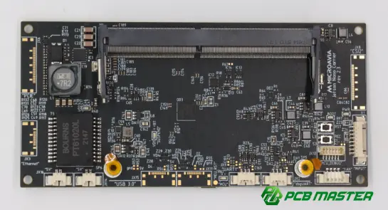
What Is a Power Inductor?
A power inductor is a passive electronic component designed to store energy in a magnetic field and control changes in electrical current. It typically consists of a coil of conductive wire or a patterned conductor combined with a magnetic core, although some designs use an air core.
Unlike signal inductors, which are often optimized for filtering, impedance matching, or high-frequency signal processing, power inductors are designed to handle relatively high currents while maintaining suitable inductance, efficiency, and thermal performance.
Power inductors are widely used in applications that require efficient energy conversion, including:
- DC-DC converters: Store and transfer energy during switching cycles in buck, boost, and buck-boost converters.
- Voltage regulators: Help maintain stable output voltage under changing load conditions.
- Battery management systems (BMS): Support power conversion and current regulation in battery-powered equipment.
- Automotive electronics: Operate in power supplies for vehicle control units, infotainment systems, and other electronic modules.
- Industrial control systems: Support motor drives, programmable logic controllers, and industrial power supplies.
- Consumer electronics: Enable compact power management in computers, smartphones, and other electronic devices.
- Telecommunications equipment: Support power delivery for communication infrastructure and networking hardware.
The appropriate power inductor depends on the electrical requirements, switching topology, operating environment, and physical constraints of the application.
How Does a Power Inductor Work?
A power inductor opposes rapid changes in current by generating a voltage in response to changing magnetic flux. This behavior follows Faraday's law of electromagnetic induction and is commonly expressed as:
V L =L(dI/dt)
Where:
- VL is the voltage across the inductor.
- L is the inductance, measured in henries (H).
- dI/dt is the rate of change of current over time.
A higher inductance produces a smaller current change for a given applied voltage and time interval, assuming the inductor remains within its intended operating range.
Energy Storage During Switching
In a typical switching converter, the power inductor repeatedly stores and releases energy.
During the energy-storage interval: When voltage is applied across the inductor, current increases and energy accumulates in its magnetic field.
During the energy-transfer interval: When the switching circuit changes state, the inductor maintains current flow by releasing stored magnetic energy into the circuit.
The energy stored in an ideal linear inductor is:
E=(1/2)LI 2
Where EEE is the stored energy in joules and III is the instantaneous current.
Because stored energy increases with the square of current, current capability is a particularly important consideration in power-inductor selection.
In practical converters, the inductor works together with switching transistors, diodes or synchronous rectifiers, capacitors, and control circuitry. Its performance therefore affects output ripple, transient response, power losses, and electromagnetic interference (EMI) .
The Role of a Power Inductor in a Buck Converter
In a buck converter, the inductor smooths the pulsating current generated by the switching stage.
When the high-side switch turns on, the voltage across the inductor drives its current upward. When the switch turns off, current continues flowing through the freewheeling path or synchronous low-side switch, and the inductor current decreases.
The resulting current waveform is typically triangular. The output capacitor works with the inductor to reduce output-voltage ripple.
For an ideal continuous-conduction-mode buck converter, the approximate inductor current ripple is:
ΔI L =(V in −V out )D/Lf s
Where:
- Vin is the input voltage.
- Vout is the output voltage.
- D is the switching duty cycle.
- fs is the switching frequency.
- L is the inductance.
For an ideal buck converter, D≈Vout/VinD\approx V_{out}/V_{in}D≈Vout/Vin. The equation assumes steady-state operation in continuous conduction mode and neglects nonideal switch and inductor voltage drops.
This relationship illustrates an important design trade-off: increasing inductance or switching frequency generally reduces inductor current ripple, but may introduce other constraints related to component size, losses, cost, and converter control.
Types of Power Inductors
Power inductors are available in several constructions, each offering different advantages in current handling, magnetic performance, size, shielding, and cost. Understanding these differences helps engineers select a component that meets both electrical and mechanical requirements.
The categories below describe common construction types. Actual performance depends on the specific component design and manufacturer specifications.
1. Shielded Power Inductors
Shielded power inductors use magnetic material or a magnetic structure around the winding to contain a greater proportion of the magnetic flux.
Key characteristics:
- Reduced external magnetic-field radiation compared with many unshielded designs.
- Often suitable for compact, high-density PCB layouts.
- Can help reduce magnetic coupling into nearby sensitive circuits.
- Available in molded metal-composite and ferrite-based constructions.
Shielded inductors are frequently used in compact DC-DC converters, automotive electronic modules, and communication equipment where electromagnetic compatibility is important.
However, shielding does not eliminate EMI. PCB current-loop area, switching-node routing, grounding, and the placement of nearby components remain important.
2. Unshielded Power Inductors
Unshielded power inductors have a more exposed magnetic field because their construction does not fully contain the magnetic flux.
Key characteristics:
- Often cost-effective for less EMI-sensitive applications.
- May offer useful current-handling capability in a relatively simple construction.
- Can be suitable for power circuits with sufficient spacing from sensitive components.
- May produce greater magnetic coupling to adjacent circuitry.
Unshielded designs can be appropriate for general-purpose power supplies and applications where cost and component availability are major considerations. Engineers should evaluate magnetic-field interaction with nearby inductors, sensors, transformers, and signal traces.
3. Molded Power Inductors
Molded power inductors typically use a winding embedded in or surrounded by a compact magnetic composite material. Many designs combine magnetic shielding with a mechanically robust package.
Key characteristics:
- Compact, mechanically robust construction.
- Potentially good magnetic shielding.
- Often available with soft-saturation characteristics, depending on the magnetic composite and design.
- Suitable for high-current, space-constrained power conversion circuits.
Molded inductors are commonly considered for processors, embedded systems, automotive electronics, and other applications requiring compact power delivery.
The term molded does not guarantee a specific saturation current, loss profile, or thermal rating. Engineers should compare actual datasheet curves rather than relying on construction terminology alone.
4. Ferrite-Core Power Inductors
Ferrite-core power inductors use a ceramic magnetic material with electrical resistivity suited to limiting certain eddy-current losses.
Key characteristics:
- Magnetic properties can be tailored to different frequency ranges.
- Often provide relatively low core losses within the intended operating conditions.
- Available in shielded and unshielded configurations.
- Commonly used in switching regulators and filtering circuits.
Ferrite-core inductors can be attractive at high switching frequencies, but their saturation behavior and loss characteristics depend on the ferrite grade, geometry, temperature, and operating flux density.
5. Wire-Wound Power Inductors
Wire-wound power inductors use conductive wire wrapped around a core or formed into a coil. They can be designed for a wide range of inductance values and current ratings.
Key characteristics:
- Flexible design options for inductance and current capability.
- Available in compact surface-mount and larger through-hole formats.
- Performance depends on wire gauge, winding geometry, core material, and thermal design.
- May require careful consideration of winding resistance and parasitic capacitance.
Wire-wound construction is used in DC-DC converters, power filters, and industrial electronics. It is a winding method rather than a mutually exclusive category: shielded, ferrite-core, and other power inductors may also be wire-wound.
Key Electrical Parameters of Power Inductors
Choosing a power inductor based only on its nominal inductance is a common design mistake. A component may meet the inductance requirement but fail under peak current, temperature, switching frequency, or transient-load conditions.
The following parameters should be evaluated together.
| Parameter | Definition | Why it matters |
|---|---|---|
| Inductance (L) | Inductive capability, measured in henries | Determines current ripple and influences converter dynamics |
| Saturation current (Isat) | Current associated with a specified reduction in inductance | Helps prevent excessive inductance loss during current peaks |
| RMS current (Irms) | Current rating associated with a defined temperature-rise limit | Indicates thermal current-handling capability under specified conditions |
| DC resistance (DCR) | Winding resistance at direct current | Determines conduction losses and contributes to heating |
| Rated operating frequency | Frequency range for which performance is characterized | Helps establish suitability for the switching application |
| Core loss | Magnetic energy dissipated in the core | Influences efficiency and component temperature |
| Self-resonant frequency (SRF) | Frequency at which inductive and parasitic capacitive effects resonate | Helps identify the limits of inductive behavior |
| Operating temperature | Permitted or characterized temperature range | Determines suitability for the thermal environment |
| Package dimensions | Physical size and footprint | Affects PCB placement, density, and thermal design |
Inductance and Current Ripple
Inductance affects the rate at which current changes. For a given applied voltage and switching interval, a higher inductance generally reduces current ripple.
However, increasing inductance may require a larger component or introduce additional winding resistance. It can also affect transient response because the inductor resists rapid changes in current.
Engineers should select inductance according to the converter topology, switching frequency, allowable ripple, load range, and control-loop requirements.
Saturation Current Versus RMS Current
These two parameters address different failure mechanisms and should not be treated as interchangeable.
Saturation current is related to the magnetic core's ability to maintain inductance as current increases. Manufacturers may specify it at a defined percentage reduction in inductance, such as 20% or 30%, but the criterion varies.
RMS current is generally related to copper loss and temperature rise under specified test conditions. The rating depends on the component's thermal environment and the manufacturer's definition.
For a converter operating in continuous conduction mode with approximately triangular inductor ripple, the peak current can be estimated as:
I peak =I out +ΔIL/2
For a buck converter, the average inductor current is approximately equal to the output current under steady-state conditions.
A suitable design must check that the peak current is compatible with the inductor's saturation behavior and that the RMS current does not cause unacceptable heating. Transient overloads, startup, and fault conditions may require additional margin.
DC Resistance and Power Loss
The approximate copper conduction loss associated with the winding is:
P DCR =I RMS 2 ×DCR
This relationship assumes DCR is evaluated at the relevant temperature and neglects additional AC winding losses.
As temperature rises, copper resistance increases, which can further increase conduction losses. At higher frequencies, skin effect and proximity effect may also increase effective winding resistance.
Therefore, a low-DCR inductor can improve efficiency, but it should not be selected without considering size, saturation current, core loss, cost, and thermal conditions.
How to Select the Right Power Inductor
A systematic selection process reduces the risk of component overheating, excessive ripple, unstable power conversion, and costly redesigns.
Step 1: Define the Electrical Operating Conditions
Establish the converter's input-voltage range, output voltage, output current, switching frequency, and topology.
For a buck converter, determine the expected inductor current ripple and peak current across relevant operating conditions. For boost and buck-boost converters, use the equations appropriate to the topology rather than applying buck-converter assumptions.
Also consider startup, load transients, minimum and maximum duty cycles, and potential fault conditions.
Step 2: Calculate the Required Inductance
Use the converter design equations to determine a practical inductance range.
For a buck converter operating in continuous conduction mode, a common initial design target is to select inductor ripple as a fraction of the rated output current. The appropriate fraction depends on the converter, load profile, transient requirements, and efficiency objectives; it is not a universal rule.
After selecting a nominal value, verify that the inductance remains adequate at peak current and over the intended temperature range.
Step 3: Verify Saturation and Thermal Margins
Check the manufacturer's inductance-versus-current curves and temperature-rise data.
Do not assume the nominal inductance remains constant at high current. Some magnetic materials exhibit gradual inductance reduction, while other designs may show more pronounced changes.
Evaluate the worst-case combination of:
- Maximum input voltage and relevant duty-cycle conditions.
- Maximum steady-state load current.
- Startup and load-transient peaks.
- Ambient temperature and local PCB temperature.
- Cooling conditions and neighboring heat sources.
The component's rated current alone does not establish whether it will operate reliably in the actual design.
Step 4: Compare Core Materials and Construction
Consider whether a shielded, unshielded, molded, ferrite-core, or other construction best fits the application.
For a high-density design near sensitive signal circuitry, magnetic shielding may be valuable. For a cost-sensitive design with sufficient spacing, an unshielded component may be acceptable.
For high-frequency operation, compare core loss, AC winding resistance, and parasitic capacitance. The best choice is determined by the complete operating profile rather than a single headline specification.
Step 5: Evaluate Size, Cost, and Availability
Confirm the package dimensions, land pattern, height restrictions, and component availability. Evaluate approved alternatives where supply continuity is important.
An electrically suitable inductor may still be unsuitable if its footprint conflicts with PCB routing, thermal requirements, mechanical clearances, or manufacturing constraints.
A complete selection process therefore includes both component-level evaluation and PCB-level design review.
PCB Layout Considerations for Power Inductors
Selecting a suitable power inductor is only part of the design process. PCB layout affects parasitic inductance, electromagnetic interference, thermal performance, and the overall behavior of the power conversion circuit.
For power electronics, the relationship between component selection and PCB implementation is particularly important.
1. Minimize High-Current Loop Area
In a switching converter, rapid current transitions can generate voltage spikes and electromagnetic interference. The layout of the input switching loop and associated return paths can significantly affect these effects.
Engineers should:
- Place the input bypass capacitors close to the switching devices.
- Minimize the area of loops carrying rapidly changing current.
- Provide short, low-impedance return paths.
- Avoid routing sensitive analog signals through noisy power-current regions.
The precise placement depends on the converter topology. A buck converter, for example, has different critical current paths from a boost converter.
2. Manage the Switching Node
The switching node connects the power inductor to the switching circuitry in many converter topologies. It can experience rapid voltage transitions and become a significant source of capacitive coupling and EMI.
Keep the switching-node copper area large enough to meet current and thermal requirements, but avoid making it unnecessarily large. Minimize its coupling to sensitive feedback, clock, and analog signal traces.
The inductor's position relative to switching devices, capacitors, and sensitive circuits should be considered during initial placement rather than left until the routing stage.
3. Design Copper and Thermal Paths Appropriately
PCB copper contributes to electrical conduction and heat spreading. However, copper thickness alone does not determine thermal performance.
Thermal behavior also depends on copper area, layer count, via placement, component losses, airflow, board geometry, and the thermal resistance of the surrounding structure.
For high-current power stages, engineers should evaluate:
- Trace width and copper thickness for allowable current and temperature rise.
- Pad dimensions and solder-joint requirements.
- Thermal vias where appropriate.
- Ground-plane continuity and return-current paths.
- Heat transfer to adjacent components and the enclosure.
Where practical, thermal simulation or measurement on a representative prototype can help validate the design.
4. Consider EMI and Magnetic Coupling
A power inductor can couple magnetic energy into nearby components and conductive loops. This is particularly important in compact PCBs containing high-speed digital circuitry, low-level analog signals, or wireless communication modules.
Shielded inductors may reduce magnetic coupling, but they do not replace good layout practices. Component spacing, orientation, current-loop geometry, grounding, and filtering should be evaluated together.
Design validation may include conducted and radiated emissions testing, depending on the product's applicable regulatory requirements.
Common Power Inductor Selection Mistakes
| Common mistake | Potential consequence | Recommended practice |
|---|---|---|
| Selecting by inductance alone | Excessive ripple, saturation, or heating | Evaluate inductance, peak current, RMS current, and losses together |
| Treating Isat and Irms as equivalent | Magnetic or thermal overload | Check the manufacturer's definitions and test conditions |
| Ignoring temperature-dependent behavior | Lower inductance or higher resistance at operating temperature | Review current and temperature derating information |
| Choosing the lowest-DCR part without other checks | Increased size, cost, or unsuitable magnetic performance | Compare total losses and electrical, thermal, and mechanical requirements |
| Using an unsuitable PCB footprint | Assembly defects or poor thermal performance | Follow the recommended land pattern and assembly guidance |
| Ignoring the switching-current loop | Increased EMI and switching noise | Optimize component placement and high-frequency return paths |
| Failing to validate load transients | Voltage deviation or excessive peak current | Test startup, load steps, and worst-case operating conditions |
These issues are often interrelated. For example, changing inductance may affect ripple and transient response, while changing the inductor package may require modifications to placement, copper geometry, and thermal design.
The practical objective is to optimize the inductor and the surrounding power stage as one system.
Power Inductor Applications Across Industries
Power inductors are used wherever electronic systems need efficient energy conversion, current regulation, or power-supply filtering. Their requirements vary with the application.
| Industry | Typical application | Key design considerations |
|---|---|---|
| Automotive electronics | DC-DC converters, onboard power supplies, electronic control units | Temperature, vibration, reliability, EMI, and automotive qualification |
| Industrial automation | Motor drives, control systems, industrial power supplies | Load variation, thermal management, and long-term reliability |
| Telecommunications | Network equipment and communication power supplies | Conversion efficiency, power density, and EMI |
| Computing | Processor voltage regulators and server power delivery | High current, transient response, and thermal performance |
| Consumer electronics | Portable devices and compact chargers | Size, efficiency, cost, and battery operating time |
| Renewable energy | Power conversion and control electronics | Current handling, temperature, efficiency, and environmental conditions |
| Medical electronics | Power supplies and embedded electronic systems | Application-specific safety, reliability, and electromagnetic compatibility |
The table identifies typical uses rather than universal component requirements. Actual selection must be based on the equipment's electrical specifications, operating environment, and applicable industry standards.
The Relationship Between Power Inductors and PCB Manufacturing
Power inductors are discrete components, but their performance depends partly on the PCB that connects them to the rest of the power conversion circuit.
A well-designed inductor can still perform poorly if the PCB introduces excessive parasitic inductance, inadequate current-carrying capacity, poor thermal paths, or unfavorable switching-node geometry.
PCB Design and Manufacturability Review
Before fabrication, engineers should verify the power-stage layout and manufacturing files. Important considerations include:
- Copper requirements: Confirm that copper thickness and conductor dimensions are suitable for the expected current and thermal limits.
- Layer stack-up: Evaluate the ground and power planes, return paths, and routing constraints.
- Component footprints: Check pad dimensions, spacing, package height, and assembly compatibility.
- Thermal design: Review heat dissipation, via structures, and the location of heat-generating components.
- EMI considerations: Inspect switching-node geometry, current-loop area, and sensitive signal routing.
- Assembly requirements: Confirm that the component package and land pattern are compatible with the intended SMT process.
These checks can identify potential problems before they become expensive prototype iterations or production defects.
How PCBMASTER Supports Power Electronics Projects
PCBMASTER provides PCB fabrication, PCBA assembly, SMT services, component sourcing, and engineering support for electronic projects across multiple industries.
For designs incorporating power inductors, these capabilities are relevant at several stages:
- Engineering file review: PCBMASTER offers free engineering file checking to identify potential manufacturability issues and provide design optimization suggestions.
- PCB fabrication: Its manufacturing capabilities support different board constructions, including multilayer PCBs and metal-core PCBs, subject to project specifications and manufacturing review.
- PCBA and SMT: Integrated assembly services support the implementation of power conversion circuits using appropriate component packages and assembly requirements.
- Quality management: PCBMASTER reports ISO 9001 and IATF 16949 certifications, as well as UL certification. Project-specific compliance should be verified against the applicable certification scope and requirements.
PCBMASTER's role is to support the manufacturing and assembly of the circuit board and electronic assembly. Power-inductor electrical characteristics, magnetic performance, and component qualification must still be verified against the selected manufacturer's datasheet and the requirements of the target application.
For engineers developing DC-DC converters, voltage regulators, or other power electronics, an early engineering review can help identify PCB-level constraints before prototype fabrication.
Frequently Asked Questions About Power Inductors
What is the difference between a power inductor and a signal inductor?
A power inductor is generally designed to handle higher current and support energy storage in power conversion circuits. A signal inductor is often optimized for filtering, impedance matching, or frequency-selective behavior in signal circuits.
The distinction is based on intended application and performance requirements rather than a universal boundary in current rating or physical size.
How do I calculate the inductance required for a power inductor?
The required inductance depends on converter topology, input and output voltages, switching frequency, duty cycle, and allowable current ripple.
For a buck converter in continuous conduction mode, the inductor ripple equation can provide an initial estimate. The resulting value should then be checked against peak current, transient response, losses, and the converter controller's requirements.
What happens if a power inductor reaches saturation?
As the magnetic core approaches saturation, its incremental inductance decreases. Current can then rise more rapidly than expected, potentially increasing switching-device stress, conduction losses, and component temperature.
Depending on the circuit, this can cause poor regulation, protection events, or component damage. Engineers should verify the inductor's inductance-versus-current behavior under worst-case operating conditions.
Does a higher inductance always improve power-conversion efficiency?
No. Higher inductance can reduce current ripple, but it may also require a larger component or introduce additional resistance and cost. Its impact on efficiency depends on core losses, winding losses, switching frequency, and the converter's operating conditions.
The optimal value balances ripple, transient response, component size, thermal performance, and total power loss.
Are shielded power inductors always the better choice?
No. Shielded designs can help reduce magnetic coupling and EMI, but they may differ in cost, size, inductance range, and loss characteristics.
The best choice depends on the circuit's electromagnetic environment, component placement, current requirements, and compliance targets.
How does PCB layout affect power-inductor performance?
PCB layout affects parasitic inductance, current paths, magnetic coupling, thermal dissipation, and EMI. Poor placement or excessive switching-loop area can cause voltage spikes, noise, and additional losses.
Correct component placement, appropriate copper design, short high-frequency current paths, and adequate thermal management help achieve the intended circuit performance.
Conclusion: Selecting and Implementing Power Inductors Effectively
Power inductors are essential components in modern power electronics, supporting energy storage, current regulation, and efficient voltage conversion. Choosing the right device requires more than matching a nominal inductance value.
Engineers should evaluate inductance, saturation current, RMS current, DCR, core losses, operating frequency, and temperature behavior together. They should also consider PCB layout, current-loop geometry, thermal paths, and electromagnetic compatibility during the design process.
For reliable results, validate the complete power stage under realistic operating conditions and review PCB manufacturability before production. Coordinating component selection, circuit design, PCB fabrication, and PCBA assembly helps reduce redesign risk and improve the consistency of the finished electronic product.
Tags: #PowerInductor #PowerElectronics #PCBDesign #DCDCConverter #VoltageRegulator #SMT #PCBA #PCBMASTER
About the Author

Carol Luo
PCB Design EngineerI'm Carol, a PCB Engineer at PCBMASTER with experience in PCB design and manufacturing engineering since 2018. I focus on translating engineering requirements into reliable PCB solutions, with expertise in stack-up design, material selection, and design-for-manufacturing (DFM). I share practical engineering insights from real-world PCB design and production experience.
Visit Carol Luo's Profile