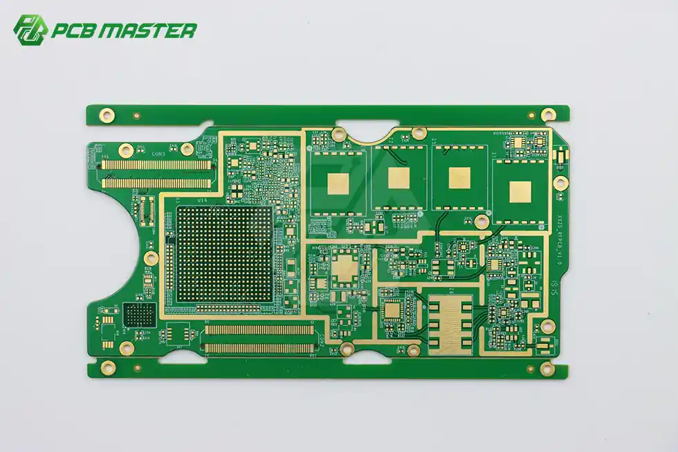
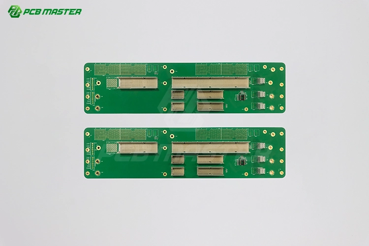
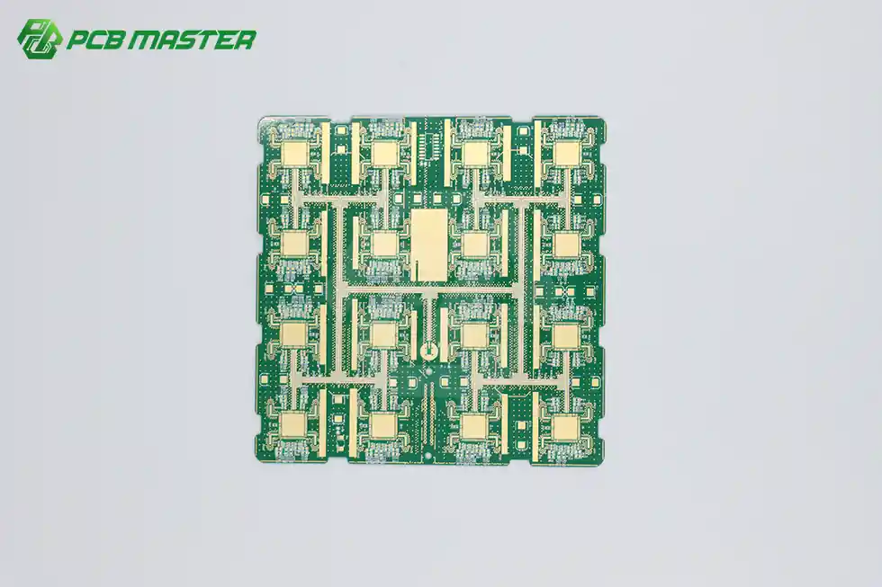
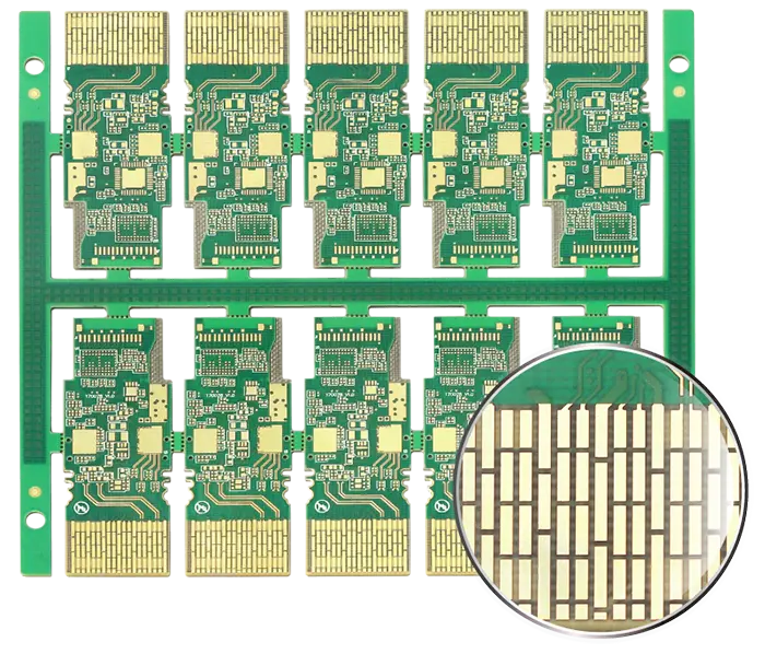
Choosing an Advanced PCB manufacturer means more than finding a supplier with advanced production capabilities. You need a partner that can understand complex requirements, communicate clearly with your engineering team, and keep your project moving efficiently from development to production.
PCBMASTER combines engineering support, complex PCB manufacturing capabilities, stable material supply, production continuity, and one-to-one technical service. This helps you reduce communication gaps, minimize unnecessary engineering changes, maintain greater consistency throughout your project, and respond more efficiently when technical issues arise.
With support from design review and manufacturing coordination to production and after-sales service, PCBMASTER provides a more connected manufacturing experience for demanding Advanced PCB projects.
An Advanced PCB is built for electronic designs where conventional board structures cannot adequately meet requirements for density, electrical performance, mechanical integration, thermal management, or manufacturing complexity.
The term does not simply refer to a high layer count. A PCB can be considered advanced because of its interconnect structure, electrical requirements, material system, mechanical construction, or combination of multiple manufacturing requirements.
Five Dimensions of Advanced PCB
01
Higher Routing Density
Fit more signal connections into a limited board area. With HDI, microvias, and other advanced interconnect processes, you can achieve more compact layouts without simply making the board larger.
02
Better Signal Performance
Support faster and more stable signal transmission. Controlled impedance, optimized stack-ups, and suitable materials help you manage signal loss, crosstalk, and other high-speed challenges.
03
More Design Freedom
Adapt the PCB to complex product structures. Multilayer, rigid-flex, and flexible constructions allow you to integrate circuits into compact or non-planar spaces.
04
Better Thermal Performance
Manage heat more effectively in high-power applications. Heavy copper, thermal vias, and metal-core structures can provide more effective paths for heat transfer.
05
Greater Manufacturing Capability
Turn demanding PCB requirements into manufacturable structures. Advanced fabrication processes and engineering control allow you to work with tighter features, more complex constructions, and demanding specifications.
Have an Advanced PCB Requirement?
Send your design files and requirements. Our engineering team will review the structure, material and manufacturing feasibility before quotation.
The level of Advanced PCB manufacturing required depends on the actual requirements of your electronic design. The goal is not to make the board unnecessarily complex, but to build a structure that can reliably meet its intended electrical, mechanical, and thermal requirements.
03 — 製品範囲
What Types of Advanced PCB Does PCBMASTER Manufacture?
PCBMASTER provides multiple Advanced PCB solutions for high-density interconnection, high-speed signals, RF applications, flexible structures, and demanding power or thermal requirements.
PCBMASTER can also support demanding PCB structures involving fine-line features, customized multilayer configurations, advanced via structures, and other application-specific manufacturing requirements.
PCBMASTER applies established quality management and compliance standards to ensure consistent Advanced PCB quality from manufacturing through final delivery.
Advanced PCB technology is used when electronic systems require higher circuit density, faster signal transmission, better thermal management, flexible form factors, or greater reliability than conventional PCB designs can provide.
Automotive & EV
Advanced PCBs support BMS, power electronics, ADAS, and vehicle control systems by providing high-density interconnections, reliable signal transmission, and thermal performance in space- and reliability-constrained vehicle environments.
電気通信
For RF, high-speed communication, and networking equipment, Advanced PCB technology supports controlled impedance, low-loss signal transmission, and dense routing required for high-frequency and high-data-rate systems.
Industrial Electronics
Advanced PCBs are used in automation, motor control, and industrial computing to integrate complex control circuits, power distribution, and communication interfaces while maintaining reliable operation in demanding industrial environments.
医療用電子機器
In medical devices, Advanced PCB technology enables compact circuit integration and reliable signal transmission where limited space, electrical stability, and consistent performance are important.
家電製品
Advanced PCBs help miniaturized products and wearable devices achieve smaller form factors by increasing circuit density and supporting flexible or rigid-flex structures for compact product designs.
航空宇宙
Advanced PCB technology supports aerospace electronics that require high reliability, lightweight construction, compact integration, and stable electrical performance under demanding operating conditions.
Ready to order an Advanced PCB for your project?
Contact PCBMASTER for one-stop engineering support, from design review and quotation to manufacturing and delivery.
Real Advanced PCB projects show how PCBMASTER applies specialized technologies to solve complex requirements in different electronic applications. The following examples highlight the project needs, key parameters, manufacturing challenges, and solutions.
A compact electronic system required higher routing density than a conventional multilayer PCB could provide. The customer needed an HDI PCB to accommodate dense component placement within a limited board area. The main challenge was completing the routing while maintaining reliable microvia structures and layer alignment. PCBMASTER optimized the HDI stack-up and manufacturing process around the layout requirements, including microvia and fine-line processing. The resulting Advanced PCB met the project's density and integration requirements.
For an RF electronic system, the customer needed stable high-frequency signal transmission and controlled electrical performance. The required High-Frequency PCB had to use suitable low-loss material and an appropriate stack-up while maintaining consistent impedance. Material selection, stack-up control, and manufacturing consistency were the main challenges. PCBMASTER coordinated the material and manufacturing requirements to achieve the specified electrical structure. The finished Advanced PCB provided the required foundation for the RF application.
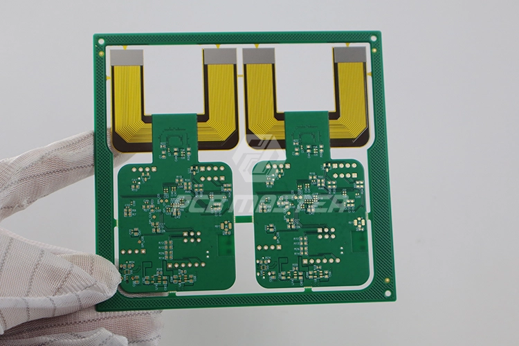
Limited installation space made conventional board-to-board connections impractical for this equipment. The customer needed a Rigid-Flex PCB that could combine rigid circuit sections with flexible areas and follow the product's three-dimensional structure. The key challenges were flexible-area reliability, accurate layer alignment, and stable lamination. PCBMASTER optimized the rigid and flexible sections according to the mechanical requirements and controlled the critical manufacturing processes. The final Advanced PCB enabled more compact integration and simplified internal interconnections.
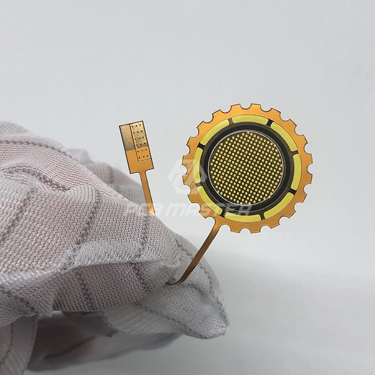
A compact electronic device required a lightweight circuit that could fit into a restricted installation area. The customer selected an FPC to provide flexible interconnection while maintaining reliable electrical performance. The main challenge was balancing the thin flexible structure with circuit reliability and manufacturing consistency. PCBMASTER selected the appropriate flexible material and controlled precision processing throughout production. The resulting Advanced PCB provided the flexibility and compact form factor required by the application.
07 — Customer Voice
Customer Reviews for Advanced PCB Projects
Customers from different industries rely on PCBMASTER for demanding Advanced PCB requirements.
“For us, the real test was what happened after the prototype. We needed the same Advanced PCB manufacturing requirements to remain under control when moving toward production. PCBMASTER was responsive when we had manufacturing questions, which made the transition much more straightforward.”
“I pay close attention to PCB material and impedance because small changes can affect RF performance. The PCBMASTER engineers understood our Advanced PCB requirements and discussed the material and stack-up with us instead of simply quoting the drawing.”
Sophie LaurentRF Design Engineer · Telecommunications · France
“Our Advanced PCB had to fit into a very limited space, so every millimeter mattered. What I valued was the engineering team's willingness to discuss the practical manufacturing constraints with us early, rather than waiting until production.”
Daniel WongProduct Development Manager · Medical Electronics · Singapore
“I don't want to spend days going back and forth over a technical question. When we raised Advanced PCB manufacturing issues, PCBMASTER's engineers responded directly and helped us work through the details. That saved quite a bit of time during development.”
ジェームズ・アンダーソンSenior Hardware Engineer · Industrial Automation · United States
08 — Start Your Project
Turn Complex PCB Requirements Into Production-Ready Results
Once you provide your Advanced PCB design files and project requirements, PCBMASTER can review the details, confirm manufacturing requirements, and prepare your quotation.
Explore practical engineering considerations to help you better understand Advanced PCB design, manufacturing, and reliability.
01
What Determines Whether Your PCB Is Truly “Advanced”?
Your Advanced PCB is not defined by layer count alone. Its complexity may come from a combination of electrical, interconnection, mechanical, thermal, and manufacturing requirements. Even if your PCB has relatively few layers, it may still require advanced manufacturing when you need tight tolerances, fine features, or specialized construction.
02
Why Can Two PCBs With the Same Layer Count Require Different Manufacturing Approaches?
When you design your PCB, layer count is only one part of the overall structure. Your trace geometry, via configuration, dielectric construction, copper distribution, material properties, and electrical requirements can all affect manufacturing complexity. As a result, two PCBs with the same number of layers may require different manufacturing approaches.
03
How Does Miniaturization Affect Your Advanced PCB Design?
As you make your electronic product smaller, you have less space for components and routing. This increases interconnection density and makes dimensional accuracy more important. Your Advanced PCB design therefore needs to consider component packaging, routing geometry, interconnection structures, and manufacturing tolerances together.
04
Why Does Copper Distribution Matter on Your Complex PCB?
When your copper distribution is uneven, it can affect etching, plating, lamination, and dimensional stability during manufacturing. By balancing copper distribution across your board, you can help achieve more consistent fabrication results and reduce the risk of manufacturing-related deformation in complex Advanced PCB structures.
05
What Role Does Thermal Expansion Play in Your Advanced PCB Reliability?
When your PCB experiences temperature changes, different materials can expand at different rates. This can create mechanical stress within multilayer structures and interconnections. If your Advanced PCB will experience temperature changes or repeated thermal cycling, you should consider the thermal expansion characteristics of the materials and board structure during design.
06
When Should You Consider Manufacturing Constraints During PCB Design?
You should consider manufacturing requirements before you finalize your PCB design. By reviewing feature sizes, tolerances, material construction, and fabrication limitations early, you can identify potential production issues sooner and reduce unnecessary design changes later.
07
Why Is Documentation Important for Your Advanced PCB Project?
Your Advanced PCB project may involve many technical variables. Clear documentation defines your intended board construction, critical dimensions, materials, electrical requirements, and acceptance criteria. This gives your engineering and manufacturing teams a consistent technical reference throughout the project.
With PCBMASTER, you can get answers to common questions about Advanced PCB design, engineering review, quotation, manufacturing, and production before you place your order.
よくある質問 高度PCB
Yes. PCBMASTER can review your design requirements and assess the manufacturing feasibility of complex Advanced PCB structures. Depending on your design, this may involve high layer counts, HDI structures, high-speed or high-frequency requirements, rigid-flex construction, heavy copper, or other specialized specifications. Our engineering team can review your manufacturing data, identify potential production concerns, and confirm the appropriate manufacturing approach before production.
You can still discuss your project with PCBMASTER before the stack-up is finalized. Provide the available design information and key requirements, such as layer count, board thickness, material requirements, impedance targets, or other critical specifications. Our engineers can review the requirements and discuss a suitable stack-up structure with you. The final stack-up should be confirmed before production to ensure that all manufacturing and electrical requirements are clearly defined.
Yes. An engineering review can be requested before placing an Advanced PCB order. PCBMASTER can evaluate your manufacturing data and identify potential issues related to board construction, fabrication requirements, tolerances, or other critical specifications. Early review can help clarify technical requirements before production and reduce the risk of changes after an order has been released.
Yes. If you know the performance and mechanical requirements but have not finalized the manufacturing structure, PCBMASTER can discuss possible manufacturing approaches with you. Our engineers can consider factors such as circuit density, electrical requirements, board construction, material availability, and manufacturing feasibility. The objective is to develop a practical Advanced PCB structure that meets your requirements without adding unnecessary manufacturing complexity.
In many cases, yes. If certain specifications are still under discussion, PCBMASTER can first review the available information and identify which open items need to be confirmed for an accurate quotation. However, changes to critical specifications such as material, layer structure, board thickness, copper, or quantity may affect the manufacturing process and final price. Open requirements should therefore be confirmed before production begins.
Cost can sometimes be reduced through engineering optimization rather than simply changing critical performance specifications. Depending on the design, this may involve reviewing the board structure, manufacturing tolerances, material options, via configuration, or panel utilization. PCBMASTER can discuss potential optimization opportunities during engineering review while keeping the project's essential electrical, mechanical, and reliability requirements unchanged.
Panelization should be considered together with the board dimensions, manufacturing process, material utilization, quantity, and assembly requirements. A suitable panel layout can improve material utilization and production efficiency while making handling and processing more practical. For an Advanced PCB, panelization may also need to account for special structures, flexible sections, or manufacturing constraints. PCBMASTER can review panelization requirements as part of the manufacturing process.
Before production approval, confirm that the key technical and commercial requirements are aligned. These typically include the final board structure, material, dimensions, thickness, copper specification, surface finish, critical tolerances, electrical requirements, quantity, testing requirements, and delivery expectations. For complex Advanced PCB projects, confirming these details before release helps ensure that the manufacturing team is working from the same final specifications.
Yes, but any change should be communicated and reviewed before production starts. Updates to material, stack-up, layer count, copper thickness, surface finish, dimensions, quantity, or testing requirements may affect engineering evaluation, manufacturing processes, lead time, or quotation. PCBMASTER can reassess the updated requirements and confirm the revised manufacturing and commercial conditions before proceeding.
Yes. PCBMASTER provides both PCB manufacturing and PCBA services, allowing customers to continue from bare PCB production to component assembly. Depending on project requirements, services can include component sourcing, SMT, THT, inspection, and testing. Using one manufacturing partner for PCB and PCBA can also simplify technical communication and coordination between board fabrication and assembly requirements.