







Inductor Voltage: Principles, Equations, and Practical Applications in Circuit Design
Inductor voltage is the voltage developed across an inductor when its current changes over time. Governed by Faraday’s law of electromagnetic induction, this relationship is fundamental to switching power supplies, DC/DC converters, filtering circuits, and energy storage systems. Understanding inductor voltage polarity, current ripple, transient response, and voltage spikes helps engineers select suitable inductors, optimize PCB layouts, and improve circuit reliability. For PCB and PCBA projects, proper inductor voltage management is essential for power integrity, electromagnetic compatibility (EMC) , and long-term performance.
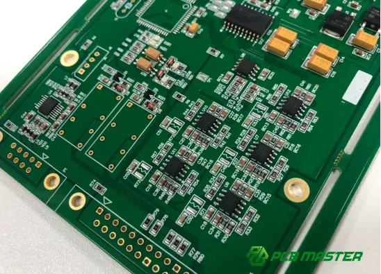
What Is Inductor Voltage?
Inductor voltage is the potential difference across an inductor caused by a changing magnetic field. When current flows through an inductor, it generates a magnetic field that stores energy. If the current changes, the magnetic field changes accordingly, inducing a voltage that opposes the change in current.
This behavior follows Lenz’s law, which states that the induced voltage acts in a direction that opposes the change responsible for producing it.
Unlike a resistor, which produces a voltage drop proportional to current, an ideal inductor produces a voltage proportional to the rate of change of current.
The fundamental equation is:
v L (t)=L[diL(t)/dt]
Where:
- vL(t) is the instantaneous voltage across the inductor, measured in volts (V).
- L is the inductance, measured in henries (H).
- diL(t)/dt is the rate of change of current, measured in amperes per second (A/s).
The sign of the voltage depends on the chosen reference polarity and current direction. Under the passive sign convention, the equation above applies directly.
Key principle: An inductor resists changes in current, not current itself. A constant current through an ideal inductor produces zero voltage across it, while a rapidly changing current can produce a large voltage.
How to Calculate Inductor Voltage
The inductor voltage equation can be rearranged to calculate inductance, current change, or the time required for a current transition.
V L =L(ΔI L /Δt)
For a constant voltage applied across an ideal inductor, the current changes linearly with time.
The following table summarizes the main equations used in engineering calculations.
| Parameter to calculate | Equation | Typical application |
|---|---|---|
| Inductor voltage | V L =L(ΔI/Δt) | Determining voltage during current transitions |
| Inductance | L=V L Δt/ΔI | Selecting an inductor for a target current ripple |
| Current change | ΔI=V L Δt/L | Estimating current ripple in switching circuits |
| Time interval | Δt=LΔI/V L | Evaluating current rise or fall time |
These simplified equations assume constant inductance and voltage over the interval. For nonlinear inductors, the effective inductance can change with current, particularly as the core approaches saturation.
Example: Calculating Inductor Voltage
Suppose a power inductor has an inductance of 100 μH, and its current increases from 0.5 A to 1.5 A in 20 μs. What voltage appears across the ideal inductor?
Step 1: Identify the parameters.
- Inductance: L=100 μH=100×10−6 H
- Current change: ΔI=1.5−0.5=1 A
- Time interval: Δt=20 μs=20×10−6 s
Step 2: Apply the equation.
V L =L(ΔI/Δt)
V L =100×10 −6 ×[1/920×10 −6 )] V
V L =5 V
The ideal inductor develops a voltage of 5 V with the reference polarity defined by the passive sign convention.
If the current decreases at the same rate, the voltage reverses polarity. This reversal is important when analyzing switching circuits and inductive transients.
What Determines the Voltage Across an Inductor?
Several electrical and physical factors influence inductor voltage in practical circuits.
1. Inductance
For the same rate of current change, a higher inductance produces a higher voltage.
For example, if the current increases at 0.1 A/μs:
| Inductance | Ideal inductor voltage |
|---|---|
| 10 μH | 1 V |
| 47 μH | 4.7 V |
| 100 μH | 10 V |
This relationship assumes constant inductance and the same current slope. A larger inductance also generally reduces current ripple when the applied voltage and switching interval remain unchanged.
2. Rate of Current Change
The current slew rate, di/dtdi/dtdi/dt, is often the most important factor in transient voltage analysis.
A slow current transition generates a relatively low voltage. A fast transition can produce a much higher voltage, even when the current change itself is modest.
In switching power supplies, the switching frequency, duty cycle, input voltage, inductance, and converter operating mode collectively determine the inductor current waveform.
3. Magnetic Core Saturation
An inductor's nominal inductance is not necessarily constant under all operating conditions. When the magnetic core approaches saturation, its effective inductance can decrease.
For a given applied voltage, a decrease in inductance produces a steeper current slope:
di L /dt=V L /L
Consequently, a saturated power inductor may experience excessive peak current, increased conduction losses, and additional stress on switching MOSFETs.
Engineers should therefore evaluate saturation current at the actual operating temperature and current waveform, rather than relying solely on the nominal inductance value.
4. Parasitic Resistance and Capacitance
A real inductor includes winding resistance, parasitic capacitance, and other nonideal characteristics. Its terminal voltage can include both inductive voltage and resistive voltage drop.
With the passive sign convention, a simplified model is:
V terminal =L(di/dt)+iR DCR
This model neglects parasitic capacitance and frequency-dependent effects. At high frequencies, these additional effects can become significant.
Inductor Voltage in DC and AC Circuits
The voltage across an inductor depends on how its current behaves over time. The distinction between DC steady state, AC operation, and transient conditions is fundamental to circuit analysis.
| Operating condition | Inductor current | Ideal inductor voltage |
|---|---|---|
| Steady-state DC | Constant | Zero |
| Increasing current | Rising | Positive under the passive sign convention |
| Decreasing current | Falling | Negative under the passive sign convention |
| Sinusoidal AC | Continuously changing | Alternates with current slope |
| Switching transient | Changes rapidly | May change rapidly in magnitude and polarity |
Inductor Voltage Under DC Conditions
When a constant DC current has reached steady state, an ideal inductor has zero voltage across it. It behaves like a short circuit in this specific steady-state model.
However, when DC voltage is first applied, the current cannot jump instantaneously in an ideal inductor. The current initially rises according to the applied voltage and inductance.
In a practical circuit, winding resistance, source impedance, and core properties determine the eventual current and losses.
Inductor Voltage Under AC Conditions
For a sinusoidal current,
i L (t)=I peak sin(ωt)
the inductor voltage is:
v L (t)=ωLI peak cos(ωt)
where ω=2πf is the angular frequency.
For an ideal inductor, voltage leads current by 90 degrees in sinusoidal steady-state operation. Its inductive reactance is:
X L =2πfL
This means that, at a fixed sinusoidal current amplitude, the required voltage increases with frequency and inductance.
It is important to distinguish this relationship from the impedance relationship V=IX L , which applies to sinusoidal steady-state phasors rather than arbitrary transient waveforms.
Inductor Voltage in DC/DC Converters
One of the most important practical applications of inductor voltage is switching power conversion. Buck, boost, and buck-boost converters use inductors to store and transfer energy between circuit nodes.
The voltage across the inductor changes as the power switch turns on and off. These voltage intervals determine the current ripple and, under steady-state conditions, the converter's voltage-conversion relationship.
Buck Converter: Step-Down Voltage Conversion
A buck converter reduces an input voltage to a lower output voltage.
During the high-side switch's on-time, the ideal inductor voltage is:
V L,on =V in −V out
During the off-time, the inductor current continues through the freewheeling path. For an ideal synchronous buck converter:
V L,off =−V out
In continuous-conduction mode (CCM) , the inductor current rises during the on-time and falls during the off-time.
For an ideal converter operating in steady state, the average inductor voltage over one complete switching period is zero. This is known as inductor volt-second balance.
Boost Converter: Step-Up Voltage Conversion
A boost converter increases an input voltage to a higher output voltage.
When the switch is on, the inductor stores energy from the input source. In the ideal circuit:
V L,on =V in
When the switch turns off, the inductor releases energy through the output path. With the stated polarity convention:
V L,off =V in −V out
Because the output voltage exceeds the input voltage, this off-state inductor voltage is negative.
The inductor current therefore rises during the on-time and falls during the off-time. The output voltage is determined by the converter topology, duty cycle, and operating conditions.
Comparing Buck and Boost Inductor Voltage
| Parameter | Buck converter | Boost converter |
|---|---|---|
| Main function | Step down voltage | Step up voltage |
| Inductor voltage during switch on | V in −V out | V in |
| Inductor voltage during switch off | −V out | V in −V out |
| Current during switch on | Increases | Increases |
| Current during switch off | Decreases | Decreases |
These equations assume ideal components and the conventional inductor voltage polarity. Actual waveforms differ because of semiconductor voltage drops, switching delays, parasitic inductance, resistance, and the converter's conduction mode.
Inductor Voltage Spikes and Transient Protection
Inductor voltage spikes occur when current is forced to change rapidly, particularly when a switching device interrupts an inductive current path.
Because an inductor resists abrupt current changes, it develops whatever voltage is required by the circuit conditions to maintain current continuity, within the limits imposed by real components and available current paths.
Excessive transient voltage can damage MOSFETs, diodes, driver ICs, and other components. It can also contribute to ringing and electromagnetic interference (EMI).
Common causes include:
- Switching a MOSFET off too quickly without an adequate current path.
- Excessive parasitic inductance in PCB traces, vias, and component connections.
- Poor placement of freewheeling diodes or snubber components.
- Large current transients during load changes.
- Magnetic saturation that causes unexpectedly high current slew rates.
Methods to Control Inductor Voltage Spikes
- Provide a suitable current path. Freewheeling diodes, synchronous switches, and clamp circuits can provide a path for inductive current when the primary switch turns off.
- Reduce parasitic inductance. Minimize high-current loop area and keep switching components and their return paths appropriately close together.
- Use snubbers or clamps when necessary. RC snubbers, RCD clamps, and TVS devices can limit specific transient conditions when selected and designed for the circuit.
- Verify component voltage ratings. MOSFETs and other switching components must withstand the expected operating voltage plus relevant transient overshoot.
- Measure the actual waveform. Use an appropriately rated oscilloscope probe and a suitable probing technique. A long probe ground lead can introduce measurement artifacts and exaggerate apparent ringing.
The correct solution depends on the converter topology, switching frequency, current level, parasitic elements, and component ratings.
How to Select an Inductor Based on Voltage Requirements
Inductor selection should consider more than the nominal inductance value. Engineers must evaluate electrical, thermal, magnetic, and mechanical requirements together.
| Selection parameter | Why it matters |
|---|---|
| Inductance | Determines current slew rate and ripple |
| Rated current | Defines the current level permitted under specified thermal conditions |
| Saturation current | Indicates where inductance begins to fall significantly under the manufacturer's defined criterion |
| DC resistance (DCR) | Affects conduction loss and temperature rise |
| Operating frequency | Influences core loss, winding loss, and effective impedance |
| Temperature rating | Determines suitability for the intended thermal environment |
| Package and footprint | Affect PCB layout, assembly, and thermal performance |
| Insulation and voltage rating, where specified | Determines suitability for electrical stress and safety requirements |
For switching converters, engineers typically calculate the required inductance from the inductor voltage, switching interval, and permitted peak-to-peak current ripple:
L=V L Δt/ΔI L
The resulting value must then be checked against the full input-voltage range, output load, switching frequency, worst-case duty cycle, saturation behavior, and thermal limits.
A component with a suitable nominal inductance may still be unsuitable if its saturation current is too low or its losses are excessive at the intended switching frequency. Manufacturer application notes from Analog Devices and Eaton provide practical examples of this selection process.
PCB Layout Considerations for Inductor Voltage
Inductor voltage is closely related to PCB layout in switching power supplies. The component itself may be correctly specified, yet poor placement and routing can increase voltage overshoot, ringing, EMI, and thermal stress.
Minimize High-Current Switching Loops
Keep the switching current loop compact, particularly the path involving the input decoupling capacitor, switching devices, and associated return connections.
Shorter, lower-inductance connections help reduce parasitic voltage spikes generated by rapid current transitions.
Control the Switch Node
The switch node in a buck or boost converter can exhibit fast voltage transitions. Avoid routing sensitive analog signals or high-impedance feedback traces close to this node.
Where appropriate, keep the switch node copper area only as large as necessary for current handling and thermal requirements. Excessive copper area can increase parasitic capacitance and electromagnetic coupling.
Optimize Grounding and Return Paths
Use a carefully planned return path for power-stage currents. Avoid forcing high-current switching returns through sensitive control-ground paths.
The grounding strategy should follow the controller manufacturer's layout recommendations, particularly for feedback sensing, current sensing, gate drive, and input bypass capacitors.
Validate the Assembled PCBA
A sound schematic and PCB layout do not guarantee correct switching behavior. Prototype validation should include inductor current ripple, switch-node overshoot, output ripple, temperature rise, and performance across operating conditions.
For demanding power electronics applications, PCB manufacturing quality, component placement accuracy, solder-joint integrity, and assembly consistency also influence the reliability of the finished product.
Common Misconceptions About Inductor Voltage
| Misconception | Correct engineering interpretation |
|---|---|
| An inductor always has a voltage across it | An ideal inductor has zero voltage when its current is constant |
| Higher inductance always means higher voltage | Voltage depends on both inductance and current slew rate |
| Inductor voltage is the same as output voltage | The voltage across the inductor depends on circuit topology and switching state |
| A higher inductance always improves converter performance | Higher inductance can reduce ripple but may affect transient response, size, cost, and losses |
| Voltage spikes occur only because of a faulty inductor | Switching behavior, parasitic inductance, current interruption, and layout can all contribute |
| Nominal inductance guarantees correct operation | Saturation, DCR, frequency-dependent losses, and temperature must also be considered |
Understanding these distinctions helps engineers avoid incorrect component calculations and diagnose power-stage problems more efficiently.
How PCBMASTER Supports PCB and PCBA Projects
Inductor voltage management is ultimately part of a broader power-electronics design and manufacturing process. PCB layout, component selection, assembly quality, and electrical testing must work together to deliver reliable hardware.
PCBMASTER provides PCB manufacturing and PCBA assembly services for a range of electronics applications, including power conversion and industrial control. Its engineering support can help customers review manufacturing files and identify potential manufacturability concerns before production.
Relevant capabilities include:
- Engineering file review: Professional technicians review submitted manufacturing files and identify potential design or production issues.
- PCB and PCBA services: PCB fabrication, assembly, component sourcing, and related engineering support are available through a one-stop service model.
- Quality management: PCBMASTER reports operating under ISO 9001 and IATF 16949 quality management systems, with UL certification.
- Prototype and production support: The company supports rapid PCB prototyping and production scheduling for different project requirements.
For a power-supply project, the engineering review should complement—not replace—electrical design verification. Engineers remain responsible for confirming inductor ratings, switching waveforms, transient protection, thermal performance, and compliance with applicable product requirements.
Conclusion
Inductor voltage is governed by a fundamental relationship: voltage equals inductance multiplied by the rate of change of current. This principle explains why an inductor can have zero voltage during steady-state DC operation but develop substantial voltage during switching and transient events.
For practical circuit design, engineers should calculate inductor voltage under the relevant operating conditions, account for saturation and parasitic effects, and select components based on ripple current, current ratings, losses, and thermal requirements. In PCB and PCBA development, careful switching-loop design, effective transient protection, and waveform validation are equally important for reliable power conversion.
The key takeaway: Reliable inductor voltage management requires coordinated electrical design, component selection, PCB layout, and hardware validation—not simply choosing an inductor with the correct nominal inductance.
Tags
#InductorVoltage #Inductor #PowerElectronics #DCDCConverter #PCBDesign #PCBA #CircuitDesign #PowerSupplyDesign #PCBMASTER
About the Author

Carol Luo
PCB Design EngineerI'm Carol, a PCB Engineer at PCBMASTER with experience in PCB design and manufacturing engineering since 2018. I focus on translating engineering requirements into reliable PCB solutions, with expertise in stack-up design, material selection, and design-for-manufacturing (DFM). I share practical engineering insights from real-world PCB design and production experience.
Visit Carol Luo's Profile