








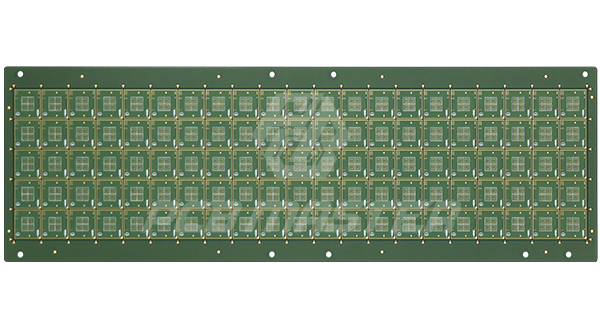
2-layer IC packaging substrate
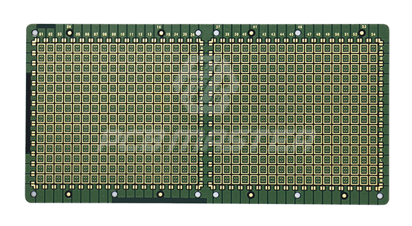
Especificaciones del producto
- Material BT
- Layer 2-layer
- Thickness 0.3mm
- Surface finish Electroless Nickel - Palladium - Gold: Nickel thickness 120 - 240U, Palladium thickness: 2U, Gold thickness: 2U
- Min Track/Spacing 0.05/0.05mm
- Special process The Subtractive process flow is adopted.
- Min hole size 0.1mm
- Special technology Small hole diameter, small trace width and trace spacing. The concentricity requirement for the circuits on both sides of the product is 0.05mm.
Productos relacionados
Listo para empezar su proyecto?
Solicite un presupuesto hoy mismo o póngase en contacto con nuestro equipo técnico para obtener asistencia.

