







What Is IPC-2221? A Complete Guide to PCB Design Requirements
The backbone of almost every electronic product, be it a smartphone, medical device, industrial equipment or automotive systems, are printed circuit boards (PCBs) . Besides connecting components, a good PCB design must also be safe, reliable, easy to manufacture and perform consistently throughout its service life. This is why PCB design standards are so important in modern electronics.
IPC family of standards offers a common set of design guidelines that assist engineers, manufacturers, and assemblers to work from the same requirements. IPC standards help teams minimize design errors, improve manufacturability, and increase the chance of a PCB to perform as intended and meet quality expectations.
The IPC-2221 is the general standard for PCB design. It covers the fundamental things like conductor spacing, trace width, material choices, mechanical design, vias, and other critical design things. Whether you’re designing a simple two-layer board or a complex multilayer PCB, IPC-2221 is a great starting point for creating designs that are both functional and manufacturable.
This guide explains what IPC-2221 is, what design requirements it covers, how to apply it during PCB design, how it compares with other IPC standards, and the common mistakes designers should avoid.
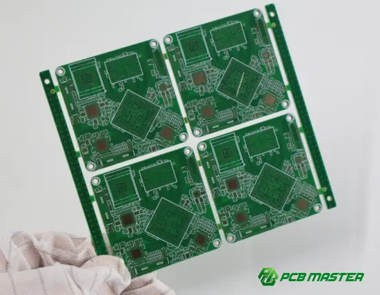
What Is IPC-2221?
IPC-2221 is the main generic standard for printed circuit board (PCB) design. It defines the minimum requirements for PCB design, such as trace width, spacing of conductors, via structure, material selection and mechanical layout rules. IPC-2221 is a “universal rulebook” for PCB design, allowing engineers to design safe, reliable and manufacturable boards for any industry and factory.
Definition of IPC-2221
IPC-2221 is the generic standard for printed circuit board (PCB) layout and construction. It defines the general requirements for printed circuit board design.
It is also the most universally applicable PCB design standard since it applies to almost every variety of PCB, from simple two-layer boards to complex multilayer PCB designs. For instance, whether a designer is developing a small IoT sensor board or an industrial control PCB, IPC-2221 provides the same baseline rules for spacing, trace routing and physical structure.
Unlike other more specialized IPC standards (for example. IPC-2152 for current carrying capacity), IPC-2221 is about general PCB design requirements. This is the reason why it is the starting point for most PCB layout guideline documentation used in PCB design software like Altium Designer or KiCad rule setup.
A real world example: If a designer is unsure what clearance to leave between two high voltage traces, IPC-2221 provides common clearance and creepage standards to reduce the chance of electrical failure or shorts.
What Is the Purpose of IPC-2221?
The IPC-2221 is mainly aimed at the standard requirements for the design of printed circuit boards so that electronic products are designed and manufactured in a consistent and reliable manner.
First, it helps to standardize PCB design rules throughout the electronics industry. If IPC-2221 did not exist, each company could use their own rules for spacing, trace widths, and via sizes. This would lead to confusion and inconsistent manufacturing results.
Secondly, IPC-2221 improves the reliability, manufacturability and safety of the device. For instance, the use of standard clearance rules can help minimize the risk of electrical arcing in high voltage circuits. The appropriate trace width guidelines can help avoid overheating in power circuits.
Third, it lowers the number of design inconsistencies from project to project. In real life PCB manufacturing one design mistake can result in expensive re-spin. With IPC-2221, this is avoided by repeatable, proven design rules that can be used and re-used across projects, such as a consumer electronics PCB or an automotive control board.
It’s like constructing bridges without common engineering standards. Thanks to IPC-2221, engineers share a standard rulebook, and the outcomes are more predictable and reliable.
Who Uses IPC-2221?
PCB designers, manufacturers and electronics companies use IPC-2221 to create consistent and manufacturable PCB designs.
PCB designers and hardware engineers use IPC-2221 to specify trace width and spacing, via size and board structure during the schematic and layout phases. For instance, if you are a PCB engineer designing a power supply board, you will leverage IPC-2221 rules to achieve safe conductor spacing and thermal performance.
IPC-2221 IPC-2221 is a standard industry guideline that helps PCB manufacturers and EMS (Electronics Manufacturing Services) providers to determine if a design can be manufactured with reasonable confidence. If a PCB layout doesn’t meet the basic spacing or hole rules, the manufacturers can reject or ask for changes before the board is fabricated.An example would be an automotive electronics company applying the rules of IPC-2221 to all control units to ensure a certain level of quality across the board.
OEMs (Original Equipment Manufacturers) use IPC-2221 in the development of electronic products to ensure design consistency across teams and suppliers.
IPC-2221 is widely used in various industries including:
- Consumer electronics (smartphone, wearables)
- Industrial automation (motor controllers)
- Automotive electronics (ECU, battery management systems) Medical devices (critical reliability)
- Aerospace systems (strict safety and performance control)
Real-life example: In the design of automotive PCBs, IPC-2221 assists in guaranteeing that the layout can endure vibration and that appropriate spacing rules are adhered to minimize the risk of failure under severe driving conditions.
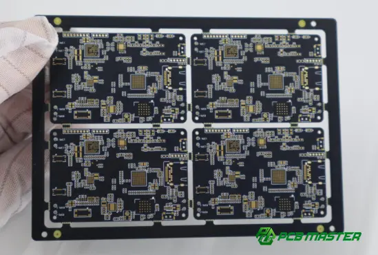
What PCB Design Requirements Does IPC-2221 Cover?
IPC-2221 describes the basic design requirements for a PCB that will result in an electrically safe, mechanically stable, and manufacturable circuit board. These requirements are used as the baseline set of rules for PCB layout including electrical behavior, physical structure, interconnections, and component placement. In practice, IPC-2221 PCB design guidelines are used in CAD tools to avoid errors prior to fabrication.
Electrical Design Requirements
IPC-2221 electrical design requirements establish rules for electrical spacing, trace sizing and current handling to ensure safety and avoid failure and overheating.
The first important rule is recommendation of trace width. This rule ensures that the copper traces can carry current safely without overheating. Take a 12V power PCB design as an example. High current paths need wider traces to avoid thermal damage.The next factor is the conductor spacing . This specifies the minimum distance between two copper traces . Sufficient spacing can prevent the occurrence of short circuits , especially in dense multilayer PCB designs used in consumer electronics .
Another important rule in high-voltage PCB design is the clearance and creepage distance. Clearance is the distance in the air between conductors, creepage is the distance along the surface of the PCB. These rules are critical for high voltage applications such as industrial power supplies to prevent electrical arcing.
Current carrying capability refers to the amount of current a trace can safely carry. In automotive PCB systems, for example, IPC-2221 current rules ensure stable operation under high load conditions such as motor control circuits.
Material and PCB Stackup Guidelines
IPC-2221 provides guidelines for PCB material selection and layer stackup definitions for electrical performance and manufacturing stability.
One is the choice of PCB substrate , or rather the choice of materials such as FR-4 , based on cost , dielectric properties , and temperature resistance . For example , in consumer electronics , FR-4 is common because it strikes a reasonable balance between performance and cost .
The next choice is copper thickness which is decided by current carrying capability and heat dissipation. For example, in power electronics like LED driver, a thicker copper is often used to carry higher current.
Besides, IPC-2221 offers a guideline for single-sided, double-sided and multilayer PCB structures. Single layer boards are used in simple devices like toys, while multilayer PCBs are used in smartphones and servers when high routing density is needed.
For example, in a 4-layer PCB design, IPC-2221 instructs the engineers on how to position the power, ground, and signal layers to reduce noise and improve stability.
Mechanical Design Requirements
IPC-2221 mechanical design requirements ensure that the PCB’s physical dimensions are correct and that it can be manufactured and assembled reliably.
First, board dimensions and outline. This defines the physical size and shape of the PCB. This is important in tight devices such as wearable electronics where space is limited.
Next up is hole size and tolerance requirements . This ensures that the drilled holes will match with the leads of the components and the mounting hardware . For example, through hole components such as connectors require tight hole size control to ensure proper soldering .
Another important requirement is copper-to-edge clearance which defines the minimum distance between copper traces and the board edge. This helps to avoid damage during routing and cutting the PCB.
Finally, considerations for mounting holes ensure that screws and mechanical supports do not interfere with electrical routing. Properly designing mounting holes in industrial control boards can help prevent failures due to vibration.
Interconnection Design Requirements
IPC-2221 interconnection requirements define how vias, pads, and connections between layers should be designed for reliability and manufacturability.
The first element is through-hole, blind, and buried vias. All layers are connected with through-hole vias. HDI PCBs use blind and buried vias to save space in smartphones and other compact devices.
Next are annular ring requirements that specify the copper ring around a drilled hole. Good annular ring ensures a strong electrical and mechanical connection and reduces the risk of open circuits.
Another important rule is the pad design recommendations , specifying the size and shape of the copper pads to solder components on . For instance , in SMT assembly , wrong pad sizing can lead to poor solder joints .
IPC-2221 via and pad rules are used in PCB fabrication checks in practice to ensure that the design can be fabricated without any defects.
Component Placement Guidelines
IPC-2221 component placement guidelines are designed to ensure electronic parts are positioned to facilitate electrical performance, thermal stability and ease of assembly.
The first rule is component spacing, which makes sure there are big enough spaces between components to avoid soldering problems and electrical interference. Rules of spacing in high density PCB designs can help to avoid soldering problems.
Next are the thermal considerations, which is the placement of heat-generating components, such as voltage regulators, away from sensitive signal components. It is a good practice to place the thermal components close to the copper pours in the power PCB design for better heat dissipation.
Finally, the assembly and manufacturability requirements ensure that the components can be readily placed by automated machines and have error free soldering. This is especially important in high-volume production settings, such as those used to produce consumer electronics.
Practical example: IPC-2221 placement rules enable designers to design compact, manageable heat and assembly efficient PCB for smartphones.
What Are the Most Important IPC-2221 Design Rules?
IPC-2221 is a set of generic PCB design rules that are used to ensure electrical safety, manufacturability and long-term reliability. These rules are generally used during the PCB layout process to avoid overheating, short circuits and fabrication problems. In practice, IPC-2221 design rules are embedded in PCB CAD tools such as Altium or KiCad to automatically enforce safe design.
Trace Width Guidelines
The IPC-2221 trace width guidelines tell us the minimum width a copper trace needs to be to safely carry electrical current without overheating.
A PCB trace is really just a wire. If it is too narrow it will overheat and fail. IPC-2221 gives guidance on the required width of traces based on current load, copper thickness, and allowable temperature rise. For example, a power PCB with 2A of current will require a much wider trace than a signal line with only milliamps of current.
In the real world of PCB design, engineers will use IPC-2221 trace width rules to layout the power paths in devices such as motor controllers or LED drivers. A common mistake is the use of a uniform trace width across the board that might lead to heating problems in high-current sections.
Conductor Spacing Requirements
IPC-2221 The Conductor Spacing Rules specify the minimum distance that must be maintained between two copper traces to avoid short circuits and electrical interference.
Spacing is very important in densely packed PCB layouts especially in multilayer PCB designs. Too close together traces can be prone to electrical arcing, or unwanted shorts during manufacturing.
For example, in consumer electronics such as smart home devices, the spacing rules of IPC-2221 help to avoid interference between high-speed signal lines, which results in better signal stability and less noise.
Clearance and Creepage Requirements
IPC-2221 establishes clearance and creepage rules for safe distances between conductive elements to prevent electrical breakdown.
Clearance is the shortest distance in air between two conductors. Creepage is the distance along the surface of the PCB. These rules are especially crucial for high voltage PCB design, e.g. industrial power supplies.
For example, in a 220V AC power board, not enough creepage distance can cause surface tracking and failure of electricity. IPC-2221 offers safe clearance between high and low voltage areas.
Via and Annular Ring Recommendations
IPC-2221 via and annular ring rules define the design of drilled holes and copper connections for reliable inter-layer connectivity.
A via links several PCB layers. IPC-2221 suggests that sufficient annular ring width (copper around the hole) should be maintained to have the mechanical strength and electrical reliability.
For instance, small vias help save room on a multilayer smartphone PCB, but IPC-2221 guarantees that even tight designs offer solid electrical connections and do not open during thermal stress.
Hole Size and Pad Design Rules
IPC-2221 hole size and pad rules define proper dimensions for drilled holes and solder pads to achieve reliable assembly and soldering.
Too small holes may not fit components well . Too small pads may cause weak or unreliable solder joints .
For example, the through-hole connectors in industrial control boards need precise hole sizes to offer good mechanical stability and strong solder joints during wave soldering.
Copper-to-Board-Edge Clearance
IPC-2221 defines copper-to-board-edge clearance as the distance copper features should be placed from the PCB edge to avoid damage during manufacturing.
In PCB fabrication, boards are cut from larger panels. If the copper is too close to the edge it could get damaged or exposed and could cause reliability issues.In automotive PCB manufacturing, proper edge clearance is a must to avoid cracking or delamination when subjected to vibration and mechanical stress.
Summary Table: Key IPC-2221 Design Rules
| IPC-2221 Design Rule | Purpose | Typical Application Example |
|---|---|---|
| Trace Width Guidelines | Prevent overheating and ensure safe current flow | Power traces in LED drivers or motor controllers |
| Conductor Spacing | Prevent short circuits and signal interference | Dense multilayer consumer electronics PCBs |
| Clearance & Creepage | Ensure safety in high-voltage designs | 220V industrial power supplies |
| Via & Annular Ring | Ensure reliable inter-layer connections | Smartphone multilayer PCB routing |
| Hole & Pad Design | Ensure strong solder joints and assembly fit | Through-hole connectors in industrial boards |
| Copper-to-Edge Clearance | Prevent edge damage during fabrication | Automotive and industrial PCB panels |
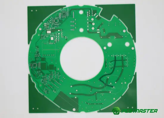
How Can Designers Ensure IPC-2221 Compliance?
The IPC-2221 compliance means that the standard PCB design rules are translated into real design constraints and are enforced by PCB CAD tools and verification steps. In practice this means that designers will need to plan requirements early, configure design rules properly and validate the layout prior to manufacturing. It decreases the number of PCB design errors, improves manufacturability, and avoids costly re-spins.
Define Design Constraints Before PCB Layout
The first step to ensure that your design will be in compliance with IPC-2221 is to establish all the electrical, mechanical and environmental constraints before you start the PCB layout.
Clear requirements help to prevent design mistakes later in the process. For example, a power PCB design for a motor controller must define maximum current, operating voltage, and temperature limits before routing starts.
Electrical requirements such as trace current capacity, voltage and signal sensitivity . Mechanical requirements such as board size, mounting holes, and enclosure restrictions . Environmental conditions such as temperature range, vibration level, and humidity exposure ( especially important in automotive PCB design ) .
A simple example: If a PCB is designed for industrial automation equipment, IPC-2221 clearance and creepage rules need to be planned early to safely handle high voltage switching.
Configure IPC-2221 Rules in PCB CAD Software
To follow IPC-2221 standards you need to configure the correct design rules within PCB CAD software like Altium Designer, KiCad, or Cadence Allegro.The width of the traces is part of the rules, and should be set according to the expected current flow. For example , power traces in a 5V 3A circuit must be thicker than signal traces to avoid overheating .
Clearance constraints define the minimum spacing between conductors. This is particularly important for high density multi-layer PCB layouts where signal integrity and safety aspects have to be considered.
The vias and pads are limited to the mechanical strength and electrical reliability of the IPC-2221 via and pad constraints for the drilled holes and copper pads . For instance, if the pad size is too small, the solder joint may fail during the assembly process.
Stackup parameters are the definition of the layer arrangement like power, ground and signal layers. A good stackup design reduces noise and improves the PCB performance in high speed designs.
Verify Compliance Using Design Rule Checks (DRC)
Design Rule Checks (DRC) are used to automatically verify if a PCB design meets IPC-2221 requirements prior to fabrication.
The electrical verification checks trace spacing, current capacity and voltage clearance to make sure the board is safe to operate. For example the DRC can find if two high voltage traces are too close and could cause arcing.
Mechanical inspection verify that holes, board edges and component placements are within the manufacturing limits. This is important to make sure that the PCB will fit into its enclosure and can be assembled correctly.
Design for manufacturability verification ensures that a PCB manufacturer can build the design. Examples are vias that are too small, or copper features that are too close to the edge of the board.
Real world example: Running DRC on consumer electronics PCBs in mass production – detects spacing violations early; reduces production defects; improves yield.
Review the Design with Your PCB Manufacturer
Always check final IPC-2221 compliance with the PCB manufacturer to be sure the design is producible.
First off you need to check what the fabricator is capable of. Fabricators have different limits of minimum trace width, via size and spacing. You need to make sure your design is within this limit to avoid rejection during the manufacturing process.Then we have Design for Manufacturability (DFM) optimization. So this is about optimizing the PCB layout for better yield, such as increasing spacing, simplifying via structures where possible, etc.
Finally manufacturability issues should be considered prior to production . For example, a manufacturer may suggest increasing clearance in high voltage sections or changing pad sizes for better soldering .
In reality, automotive and medical PCB projects undergo multiple design review cycles with the manufacturer to ensure full IPC-2221 compliance and long term reliability.
How Is IPC-2221 Different from Other IPC Standards?
IPC-2221 is a general standard for PCB design, while other IPC standards address specific areas like rigid board construction, current calculation, footprint design, manufacturing acceptance, etc. Simply put, IPC-2221 defines “basic design rules”, but it does not substitute specialized standards that are used for detailed PCB engineering decisions.
IPC-2221 vs. IPC-2222
IPC-2221 describes the general requirements for PCB design, whereas IPC-2222 describes the specifics for the construction of rigid PCBs.
IPC-2221 is a generic standard for all PCB types (single and multilayer boards) and includes generic rules such as spacing, trace width and basic layout safety.
In contrast, IPC-2222 offers a more in-depth look at rigid printed circuit boards. It provides a more complete coverage of structural design, materials use and construction details than IPC-2221.
For example, an engineer building a typical consumer electronics PCB might use IPC-2221, but IPC-2222 provides additional structural guidance for building a rigid PCB for industrial control systems that needs to be highly reliable.
IPC-2221 vs. IPC-2152
IPC-2221 gives general conductor guidelines whereas IPC-2152 is used for more accurate trace current and thermal calculations.
IPC-2221 has basic trace width recommendations based on simplified assumptions. Good for general layout rules and early PCB design.
This is mitigated by IPC-2152. This document provides detailed thermal and electrical models to determine the safe current carrying capacity of a PCB trace under real operating conditions.
But for example in a power PCB design, such as a motor driver board, you would typically use IPC-2152 to calculate accurate trace widths, and IPC-2221 as a general starting point.
IPC-2221 vs. IPC-7351
IPC-2221 covers generic PCB design rules whereas IPC-7351 covers standard land patterns (footprints) for components.
IPC-2221 includes general PCB layout rules, such as spacing, vias, and structural design.
IPC-7351 describes how to create footprints for components such as resistors, capacitors, and IC pads. IPC-7351 provides a common land pattern for PCB designs and PCB manufacturers.
For instance, IPC-7351 defines the pad shape and size for laying down a QFN package IC, while IPC-2221 defines appropriate spacing between that IC and adjacent components.
IPC-2221 vs. IPC-6012
IPC-2221 sets the requirements for PCB design. IPC-6012 sets the performance and acceptance criteria for manufactured PCBs.
During the design process, the IPC-2221 is used to make sure that a PCB is properly designed and manufacturable.
After the PCB is manufactured, the IPC-6012 is used to check that the completed PCB fulfills the requirements for quality and reliability.
- IPC-2221 : This is useful during the design process to indicate proper spacing and trace width .
- IPC-6012 : This is used by manufacturers for inspection of the finished board for defects ( delamination , conductor issues , etc . ) .
Comparison Table: IPC Standards Overview
| IPC Standard | Primary Focus | Typical Use |
|---|---|---|
| IPC-2221 | General PCB design requirements | General PCB design |
| IPC-2222 | Sectional design requirements for rigid PCBs | Rigid PCB design |
| IPC-2152 | Trace current capacity and thermal modeling | Power and thermal design |
| IPC-7351 | Standard PCB land patterns (footprints) | Component footprint design |
| IPC-6012 | PCB performance and acceptance standards | PCB fabrication and quality inspection |
When Should Multiple IPC Standards Be Used Together?
In PCB design for general and specialized engineering requirements, more than one IPC standard needs to be used together.
In practice, engineers don’t use a single standard for PCB projects, they often use IPC-2221 as the basic reference and add other standards based on the complexity of the design.
For example, a power electronics PCB could employ IPC-2221 for general layout rules, IPC-2152 for accurate current calculations, and IPC-6012 for the final acceptance criteria for manufacturing.
IPC-2221 for safe spacing IPC-7351 for component footprints IPC-2222 for details on rigid board construction.
What Are the Common Mistakes When Using IPC-2221?
It is a basic standard in PCB design but many design problems still occur due to improper or incomplete application by engineers. Most of these mistakes come from a lack of understanding of its purpose, not taking into consideration the actual manufacturing constraints, or using old or unverified design rules. These errors can lead to PCB failures, higher costs and redesign efforts.
Treating IPC-2221 as the Only PCB Design Standard
It’s a common mistake to consider IPC-2221 as the only reference for PCB design instead of combining it with other IPC standards.
IPC-2221 gives general PCB rules for design but does not cover all detailed engineering needs. For example, it does not include complete definition of precise trace current calculation or detailed footprint standards.
In actual PCB design engineers should also use IPC-2152 for accurate current handling and IPC-7351 for component land patterns. If a designer only adheres to IPC-2221 they can miss critical details that impact performance.
For example, in a high-speed communication board, a design based on IPC-2221 alone may result in improper impedance control or thermal problems.
Ignoring PCB Manufacturer Capabilities
Yet another mistake that is often made is designing a PCB with no regard to the actual manufacturing limits of the PCB supplier.
Even though a design meets the IPC-2221 rules, the design may fail if it is beyond what the manufacturer can manufacture. For instance, very small trace widths or tight spacing may not be supported by low cost fabrication processes.
Many PCB manufacturers have their own minimum trace width, via size and copper spacing limits. Not adhering to these limits will lead to rejected designs or costly production changes.
For example, if you design your prototype board with very tight spacing, and the chosen manufacturer cannot achieve that level of precision, you may have to redo the board.
Misunderstanding Clearance and Creepage Requirements
Many design errors are the result of misunderstanding the clearance and creepage distance rules in IPC-2221.
Clearance is the shortest air distance between conductors, and creepage is the distance along the PCB surface. Both are important for high-voltage PCB safety.
A common mistake is to check only for clearance and ignore creepage, which can lead to surface tracking failures under humidity or contamination conditions.
For instance, if the creepage distance is not sufficient on an industrial power supply board, electrical leakage can occur on the surface of the PCB even if the air gaps are correct.
Applying Generic Design Values Without Validation
A common design mistake is to use default or generic IPC-2221 values without validating actual operating conditions.
IPC-2221 covers baseline recommendations but real designs depend on real voltage, current, temperature and environment. If designers apply values blindly, PCB may not perform safely under real conditions.
For instance, a trace width not designed with heat dissipation in mind can overheat in a high current automotive PCB.
A better way is to validate the IPC-2221 rules with real application requirements such as load current and ambient temperature.
Using Outdated Versions of IPC-2221
Using old IPC-2221 documentation can result in wrong or incomplete PCB design rules.
The IPC standards are updated over time to include new materials , manufacturing capabilities , and design practices . Older versions may not reflect current best practices in the industry .
For example, the newer PCB fabrication technologies may offer tighter tolerances than older IPC recommendations, or improved safety guidelines for high density designs.
A classic example would be designers working in automotive or aerospace industry who must make sure they always work with the latest IPC-2221 revision in order to avoid compliance issues and manufacturing risks.
Conclusion
IPC-2221 is the baseline standard for PCB design and contains important rules for trace width, spacing, vias and the overall board structure. When IPC-2221 PCB design requirements are followed, engineers are able to build circuits that are safer, more reliable and easier to manufacture across industries from consumer electronics to automotive and industrial systems.But IPC-2221 alone does not fully address the design of a PCB. It is best used in conjunction with other IPC standards to ensure electrical performance, footprint and full manufacturing compliance in real-world engineering applications. This multi-pronged approach reduces design uncertainty and improves the quality of the product.Most importantly, early verification of IPC-2221 compliance in the design process can go a long way toward reducing expensive redesigns, production delays and manufacturing defects. Simple verification steps during PCB layout often can mean the difference between a smooth production run versus repeated iterations.For example, PCBMASTER applies the IPC-2221 guidelines in practice , along with rigorous manufacturing verification, to guarantee that each PCB design meets the real-world needs of production. PCBMASTER combines the design standards with fabrication capabilities to help ensure consistent quality and reliable performance for complex PCB and PCBA projects.
FAQ
What is the latest version of IPC-2221?
The current general standard for PCB design fundamentals is the widely accepted revision of IPC-2221, IPC-2221B (updates and associated revisions are dependent on IPC release cycles). This revision contains updated guidance on spacing, trace design and manufacturability considerations.
It is important to use the latest edition of IPC-2221 because the manufacturing technologies, materials and density requirements of PCBs are constantly changing. New revisions include the latest industry knowledge such as improved high-density layout techniques, safety margins and matching current fabrication capabilities. For example newer versions define newer PCB stackups and tighter manufacturing tolerances versus older releases.
Is IPC-2221 mandatory for PCB manufacturing?
IPC-2221 is not a universal requirement, but is required when specified in customer specs or contracts, or when required by industry standards.
In practice, the IPC standards are normally viewed as recommendations and not as legally binding standards by the PCB manufacturers. However, in certain sectors, such as automotive, aerospace and medical electronics, IPC standards are frequently incorporated into the product specifications. For example, an automotive OEM might specify that all PCB designs must comply with IPC-2221 standards in order to meet safety and reliability in demanding environments.
In summary, IPC-2221 is a recommended practice in general but becomes a required standard when specified in engineering contracts or in regulated industries.
Can IPC-2221 be used for HDI and high-speed PCB designs?
IPC-2221 is a good standard to follow for your HDI and high speed PCB designs, but it is a general baseline standard not a complete design solution.
General rules for spacing, vias and layout safety for HDI (High-Density Interconnect) PCBs are provided by IPC-2221. However, many HDI designs need to adhere to additional standards that cover microvias, fine pitch routing and advanced stackup structures.
IPC-2221 alone is not sufficient for high speed PCB design. It is usually used in conjunction with other high speed design practices such as impedance control rules, signal integrity analysis and material selection. For example, in a high-speed communication board, IPC-2221 helps ensure safe spacing, while other engineering rules manage signal timing and noise control.
Can small PCB projects benefit from IPC-2221?
Yes, IPC-2221 is still very useful for small PCB projects even in prototype or low volume production.
One of the things that is in IPC-2221 are a set of design rules that prevent common errors like wrong trace widths, spacing and via design. Such errors can cause problems such as overheating, shorts, bad soldering, even on simple prototype boards.
Even a simple little Arduino control board benefits from the IPC-2221 because that means there will be enough spacing and trace sizing to reduce the likelihood of failure when the board is tested or produced in small quantities.
In short, IPC-2221 makes designs more reliable at every level, from prototype to mass production.
Where can I obtain the official IPC-2221 standard?
The official IPC-2221 standard can be purchased directly from the IPC (Association Connecting Electronics Industries) official website or from authorized distributors.
IPC documents are controlled technical standards. Unofficial copies may not be current, complete or accurate. Use of incorrect versions may result in design errors or non-conformance in regulated industries.
The official standard for engineering teams. Purchase it and you will have the latest revisions, the correct technical definitions and the legal backup for professional work on PCB design.
About the Author

Carol Luo
PCB Design EngineerI'm Carol, a PCB Engineer at PCBMASTER with experience in PCB design and manufacturing engineering since 2018. I focus on translating engineering requirements into reliable PCB solutions, with expertise in stack-up design, material selection, and design-for-manufacturing (DFM). I share practical engineering insights from real-world PCB design and production experience.
Visit Carol Luo's Profile