







Impedance of Inductor: Formula, Frequency Dependence, and PCB Design Considerations
The impedance of an inductor is frequency-dependent and is commonly expressed as Z = R + jωL , where R represents resistance, L is inductance, and ω is angular frequency. For an ideal inductor, the impedance magnitude increases linearly with frequency according to |Z| = 2πfL . In practical PCB circuits, however, winding resistance, parasitic capacitance, self-resonant frequency (SRF) , and material characteristics all affect the actual impedance. Understanding these factors is essential when selecting inductors for power conversion, filtering, RF circuits, and other PCB applications.
What Is the Impedance of an Inductor?
An inductor opposes changes in current by generating a magnetic field. Its electrical impedance describes how strongly it resists an alternating current at a particular frequency.
For an ideal inductor , impedance is:
ZL =jωL=j2πfL
where:
- ZL = inductive impedance
- j = imaginary unit
- ω = angular frequency in rad/s
- f = frequency in Hz
- L = inductance in H
The magnitude is:
∣ZL ∣=2πfL
This means that an ideal inductor has increasing impedance as frequency increases .
For example, a 10 µH ideal inductor has:
| Frequency | Ideal Inductive Impedance |
|---|---|
| 100 Hz | 6.28 mΩ |
| 1 kHz | 62.8 mΩ |
| 10 kHz | 0.628 Ω |
| 100 kHz | 6.28 Ω |
| 1 MHz | 62.8 Ω |
The relationship is straightforward: doubling the frequency doubles the ideal inductive reactance .
Inductor Impedance Is Not Purely Inductive in a Real Circuit
A practical inductor contains more than inductance. Its winding has DC resistance, and its physical construction introduces parasitic capacitance.
A simplified practical model can therefore be represented as:
Z≈R ESR +jωL
at frequencies sufficiently below the component's self-resonant frequency.
Here, RESR represents the equivalent series resistance of the winding.
This distinction matters when an inductor is used on a PCB. The datasheet inductance alone does not fully describe its high-frequency behavior.
DC Resistance
The winding resistance produces real power loss:
P=I2 R
Higher current therefore increases conduction losses and can raise component temperature.
Parasitic Capacitance
Adjacent turns, pads, terminals, and other structures create small parasitic capacitances. At sufficiently high frequency, these capacitances become increasingly important.
Eventually, the inductor reaches its self-resonant frequency (SRF) .
What Happens at the Self-Resonant Frequency?
An actual inductor can be approximated using an inductance in combination with parasitic capacitance. Its approximate self-resonant frequency is:
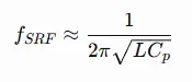
where Cp represents the effective parasitic capacitance.
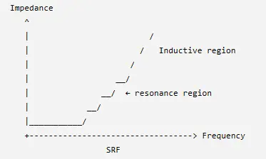
Below the SRF, the component generally behaves predominantly as an inductor.
At the SRF, the inductive and capacitive effects interact strongly, producing a resonance.
Above the SRF, the component can behave predominantly capacitively rather than inductively .
This is one of the most important reasons engineers should not assume that an inductor's nominal value determines its impedance at every frequency.
Typical Impedance Behavior
How to Calculate Inductor Impedance
For an ideal inductor, use:
ZL =2πfL
Example
Suppose:
- L = 10 µH
- f = 100 kHz
Then:
XL =2π(100,000)(10×10 −6 )
XL ≈6.28Ω
Therefore, the ideal inductive reactance is approximately 6.28 Ω .
If the inductor has a series resistance of 0.2 Ω, its simplified impedance becomes:
Z=0.2+j6.28Ω
and its magnitude is approximately:

At this frequency, the inductive component dominates the magnitude.
Inductor Impedance vs. Frequency
Frequency is one of the most important variables when selecting an inductor.
| Frequency Region | Dominant Behavior | Design Consideration |
|---|---|---|
| Low frequency | Inductive + winding resistance | Check DCR and current rating |
| Mid-frequency | Predominantly inductive | Verify inductance and impedance |
| Near SRF | Resonant behavior | Check impedance curve carefully |
| Above SRF | Increasingly capacitive | Do not treat the component as an ideal inductor |
What Determines the Practical Impedance of an Inductor?
1. Inductance Value
A higher inductance produces higher inductive reactance at the same frequency:
XL ∝L
However, selecting the highest possible inductance is not automatically the correct design decision. Current rating, saturation characteristics, DCR, physical size, and frequency range must also be considered.
2. Operating Frequency
Because:
XL =2πfL
the same inductor can exhibit dramatically different impedance at different frequencies.
An inductor that provides only a small impedance at a low switching frequency can provide substantially higher impedance to higher-frequency noise components.
3. DC Resistance
DCR contributes to power dissipation and voltage drop. For power applications, engineers should evaluate:
- DCR
- Rated current
- Saturation current
- Temperature rise
- Core losses
4. Core Material and Construction
The magnetic core and winding structure influence inductance, losses, frequency response, and saturation behavior.
For high-frequency applications, the physical construction of the component becomes increasingly important because parasitic effects cannot be ignored.
5. Self-Resonant Frequency
The SRF determines the frequency range in which the component can effectively behave as an inductor.
A component intended for high-frequency filtering should therefore be evaluated using its impedance-versus-frequency curve , rather than only its nominal inductance.
Inductor Impedance in PCB Applications
Inductors are widely used in PCB designs, including:
- DC/DC converters
- LC filters
- EMI filters
- Power supply circuits
- RF matching networks
- Oscillators
- Signal filtering
- Common-mode filtering
- Energy-storage circuits
For example, in a switching regulator, the inductor stores and releases energy as the switching waveform changes. Its inductance, current rating, DCR, core characteristics, and frequency response directly affect converter performance.
For an RF circuit, however, the designer may be more concerned with the component's impedance curve, Q factor, SRF, and parasitic elements.
The same nominal inductance value can therefore have very different practical performance in different PCB applications.
Common Mistakes When Working With Inductor Impedance
Mistake 1: Treating the Inductor as an Ideal Component
Using only:
Z=j2πfL
may be insufficient for high-frequency design.
Better approach: Check the manufacturer's impedance, Q-factor, SRF, DCR, and frequency characteristics.
Mistake 2: Ignoring SRF
An inductor does not remain inductive indefinitely as frequency increases.
Better approach: Ensure the operating frequency and significant harmonic content remain appropriate for the selected component.
Mistake 3: Selecting an Inductor Based Only on Inductance
A 10 µH component is not automatically equivalent to another 10 µH component.
Their DCR, saturation current, core material, package, SRF, and loss characteristics may differ substantially.
Mistake 4: Ignoring PCB Layout
At high frequencies, PCB traces, vias, pads, and component placement contribute additional parasitic inductance and capacitance.
For high-frequency PCB designs, engineers should therefore consider the component and PCB interconnect as part of the same electrical system .
How Should Engineers Select an Inductor for PCB Design?
A practical selection process can include the following steps:
- Define the operating frequency range.
- Determine the required inductance.
- Calculate the expected inductive reactance.
- Check maximum RMS and peak current.
- Check DCR and associated power loss.
- Review the saturation characteristics.
- Verify the self-resonant frequency.
- Review impedance and Q-factor curves from the manufacturer.
- Evaluate PCB footprint and thermal requirements.
- Validate the final design under actual operating conditions.
PCBMASTER's Perspective on Inductor-Related PCB Design
For PCB projects involving inductors, the component itself is only one part of the electrical design. PCB layout, material selection, stack-up, routing, thermal management, and manufacturing tolerances can all affect circuit behavior.
PCBMASTER supports PCB and PCBA projects across different application requirements, including standard, high-frequency , HDI , rigid-flex , FPC , and other advanced PCB structures. Its engineering team provides free engineering file review to identify potential manufacturability, performance, and cost issues before production.
For high-frequency PCB projects in particular, PCBMASTER reports production capacity of 50,000 items/month , while its broader manufacturing capabilities include HDI, rigid-flex, FPC, and metal-core PCBs. These capabilities can be relevant when an inductor is part of a high-speed, RF, power-management, or thermally demanding PCB design.
The engineering review should consider not only whether the component fits the footprint, but also whether the surrounding layout supports the intended electrical and thermal performance.
Key Takeaways
The impedance of an ideal inductor is determined by:
ZL =j2πfL
and its magnitude is:
∣ZL ∣=2πfL
The key point is that inductor impedance increases with frequency only within the component's effective inductive operating range . In a real component, DCR, parasitic capacitance, core losses, Q factor, and SRF significantly influence actual behavior.
For PCB design, engineers should therefore evaluate the complete impedance-versus-frequency characteristics of the selected component , rather than relying solely on its nominal inductance value.
Tags: #InductorImpedance #Inductor #PCBDesign #PCBA #SMT #PowerElectronics #RFDesign #HighFrequencyPCB #CircuitDesign #PCBMASTER
About the Author

Carol Luo
PCB Design EngineerI'm Carol, a PCB Engineer at PCBMASTER with experience in PCB design and manufacturing engineering since 2018. I focus on translating engineering requirements into reliable PCB solutions, with expertise in stack-up design, material selection, and design-for-manufacturing (DFM). I share practical engineering insights from real-world PCB design and production experience.
Visit Carol Luo's Profile