








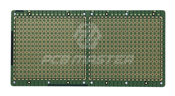
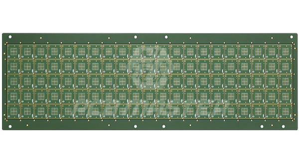
2-layer IC packaging substrate
Produktspezifikationen
- Material BT
- Layer 2-layer
- Thickness 0.3mm
- Surface finish Electroless Nickel - Palladium - Gold: Nickel thickness 120 - 240U, Palladium thickness: 2U, Gold thickness: 2U
- Min Track/Spacing 0.05/0.05mm
- Special process The Subtractive process flow is adopted.
- Min hole size 0.1mm
- Special technology Small hole diameter, small trace width and trace spacing. The concentricity requirement for the circuits on both sides of the product is 0.05mm.
Verwandte Produkte
Bereit, Ihr Projekt zu starten?
Holen Sie sich noch heute ein Angebot oder Kontakter technisches Team für Unterstützung.

