








Technical Guide for Multilayer FPC Engineering High-Density Interconnects and Reliability Optimization
I. Core Challenges and Technological Breakthroughs in Multilayer FPC
1. Multilayer FPC (4+ layers) achieves 10× higher wiring density than single-sided boards but faces three critical challenges:
2. Layer Misalignment : ±25μm registration errors cause micro-shorts (Source: IPC-6013D 4.4.2)
3. Z-Axis Stress : Interlayer separation force >8N/mm² during bending (Fujifilm 2024 Test)
4. Impedance Deviation : ±10% tolerance triggers signal integrity failure
Industry Pain Point : Traditional 4-layer FPC yield remains 65–75% (2023 Shenzhen FPC Factory Report), while 6+ layer FPC costs surge by 40%.

II. High-Reliability Design Specifications (with Computational Models)
1. Stackup Architecture Optimization
| Layers | Material Stack | Thickness Tolerance | Applications |
|---|---|---|---|
| 4-Layer | PI Base + 2L Cu Foil + Acrylic Adhesive | ±8% | Smartphone Camera Modules |
| 6-Layer | Modified PI + 18μm Ultra-Thin Cu + Adhesiveless Lamination | ±5% | Satellite Foldable Antennas |
| 8-Layer | LCP (Liquid Crystal Polymer) + mSAP Process | ±3% | Impla |
Key Formula: Impedance Control

- Note: W=Trace Width (μm), H=Dielectric Thickness (μm), T=Copper Thickness (μm), ε_r=Permittivity (PI=3.2, LCP=2.9)*
2. Via Technology Comparison
| Type | Min. Hole Size/Aspect Ratio | Reliability Limit | Cost Increase |
|---|---|---|---|
| Mechanical Drilling | ≥100μm / 1:8 | Fracture after 500 thermal cycles | Baseline |
| Laser Ablation | 30–50μm / 1:3 | Survives 2,000 bend cycles | +15% |
| Plasma Etching | 15–25μm / 1:1.5 | Optimal for 8-layer FPC | +35% |
Case Study : Huawei’s 6-layer FPC foldable screen cable uses stepped laser vias, reducing bend radius to 0.3mm (2023 Patent CN114928649A).
III. Five Critical Manufacturing Control Points
1. Lamination Process
① Vacuum hot-pressing: 185°C ±5°C, 12MPa, 60min dwell (Toray CB-Series PI)
② Resin flow control: 120–150μm range (prevents thickness variation)
2. Copper Surface Treatment
① Ultra-thin Cu foil: 2μm electroless copper + 5μm electroplated Cu (Ra roughness <0.8μm)
② Interlayer adhesion: >1.8N/mm (ASTM D903)
- Precision Etching
Alkaline etchant formula:
① Cu²⁺ concentration: 120–140g/L
② NH₃·H₂O: 8–10mol/L
③ Temperature: 50°C ±2°C → 88–89° sidewall angle
4. Coverlay Integration
① Dynamic zones: 25μm modified PI coverlay + laser ablation (±7μm accuracy)
② Pad zones: Prepreg via fill (voiding <5%)
IV. Reliability Validation Framework (per JEDEC/IPC)
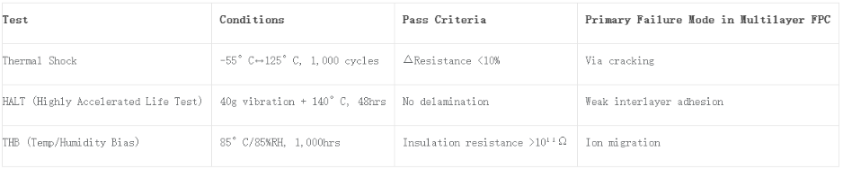
- Data Sources: IPC-6013D Class 3 / NASA-EEE-INST-002*
V. Application Decision Tree

VI. Technology Evolution Trends
1. Material Innovation : Nano-ceramic-filled PI reduces CTE to 8ppm/°C (Panasonic 2024)
2. Process Revolution : Roll-to-Roll (R2R) production cuts 8-layer FPC cost by 28% (Samsung Display Roadmap)
3. Integration Breakthrough : Embedded passive components shrink 8-layer FPC volume by 40% (Apple Vision Pro)
Conclusion
Multilayer FPC has evolved from interconnects to high-density system solutions. For 5G mmWave and brain-computer interfaces, alignment accuracy must break the ±15μm barrier, while dielectric loss must be suppressed below 0.002. Synergizing material science, precision manufacturing, and AI process control will unlock the full potential of multilayer FPC .
Engineer Alert : For >6-layer multilayer FPC , adopt mSAP processes and 3D AOI inspection—otherwise yields drop below 55% (Flexium 2023 Report).
About the Author

Jack Wang
Production DirectorI'm Jack Wang, Production Director at PCBMASTER, responsible for PCB manufacturing and SMT assembly operations since 2014. My focus includes production management, yield optimization, cost control, and lean manufacturing across PCB fabrication and SMT processes. I share practical insights from real-world PCB mass production and factory operations.
Visit Jack Wang's Profile


