







Inductor Symbol: Meaning, Types, and How to Read It in Circuit Diagrams
The inductor symbol is a standardized circuit-diagram representation of an inductor, typically shown as a series of curved loops or a rectangular coil symbol. Understanding the symbol helps engineers identify inductors, distinguish fixed and variable types, interpret polarity and core information, and correctly analyze PCB schematics. This guide explains common inductor symbols, their meanings, applications, and practical considerations when selecting components for PCB and PCBA designs.
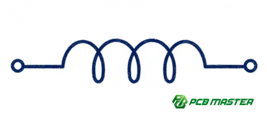
What Is an Inductor Symbol?
An inductor symbol is the graphical representation used to identify an inductor in an electrical schematic. An inductor is a passive component that stores energy in a magnetic field when current flows through its winding.
The most common inductor symbol consists of a series of curved loops:
—((((—
The exact graphical appearance can vary depending on the schematic standard, software, region, and component type. However, the fundamental purpose remains the same: to indicate that the component provides inductance in the circuit .
The electrical unit of inductance is the henry (H) . Practical electronic circuits commonly use:
- µH — microhenry
- mH — millihenry
- nH — nanohenry
For example, an inductor marked 10 µH has a nominal inductance of 10 microhenries.
Why Is the Inductor Symbol Important?
A schematic is a functional representation of an electronic circuit rather than a physical representation of the PCB. The inductor symbol allows engineers to identify the component's electrical function without showing its actual package.
The same electrical inductor could physically appear as:
- A wire-wound through-hole component
- A surface-mount chip inductor
- A power inductor
- A molded inductor
- A shielded inductor
- A high-frequency RF inductor
The schematic symbol provides the electrical information, while the BOM, datasheet, footprint, and PCB layout define the physical implementation.
Common Types of Inductor Symbols
Different inductor constructions and functions may use different schematic symbols.
Fixed Inductor Symbol
The standard fixed inductor symbol represents an inductor whose nominal inductance is fixed.
It is commonly used in:
- DC/DC converters
- Power supply filtering
- EMI filtering
- RF circuits
- Signal filtering
- Energy storage circuits
The schematic may place an inductance value next to the symbol, such as 4.7 µH , 10 µH , or 100 nH .
Variable Inductor Symbol
A variable inductor is generally represented by the standard inductor symbol with an arrow indicating that its inductance can be adjusted.
Variable inductors can be used in applications requiring tuning, including certain:
- RF circuits
- Resonant circuits
- Oscillators
- Matching networks
- Tuning circuits
The symbol distinguishes the adjustable component from a conventional fixed-value inductor.
Inductor With Magnetic Core
Some schematic conventions add lines near the inductor winding to indicate a magnetic core.
The additional lines communicate that the inductor uses a magnetic material as part of its construction.
Core material can significantly influence:
- Inductance
- Saturation behavior
- Energy storage
- Magnetic losses
- Frequency response
This distinction can therefore be important when interpreting a power or magnetic circuit.
Coupled Inductors
When two or more inductive windings share magnetic coupling, the schematic normally shows multiple coils positioned close to each other, with core or coupling markings where applicable.
This representation is commonly encountered in:
- Transformers
- Coupled inductors
- Isolated power supplies
- Common-mode chokes
- Signal isolation circuits
The relative arrangement and polarity markings help engineers understand the magnetic relationship between the windings.
Inductor Symbol vs. Other Passive Component Symbols
Inductors are often encountered alongside resistors and capacitors, so recognizing the differences between their symbols is fundamental when reading a schematic.
| Component | Typical Symbol Concept | Primary Function | Common Unit |
|---|---|---|---|
| Resistor | Zigzag or rectangular element | Limits current / creates voltage drop | Ω |
| Capacitor | Two parallel plates | Stores electric-field energy | F |
| Inductor | Coil or looped winding | Stores magnetic-field energy | H |
| Transformer | Coupled coils | Transfers energy between windings | H / VA |
The inductor symbol represents magnetic energy storage , whereas the capacitor symbol represents electrical energy storage.
How to Read an Inductor on a Schematic
Recognizing the symbol is only the first step. Engineers normally need to interpret the information associated with it.
1. Identify the Inductance Value
The schematic may specify a nominal value such as:
L1 = 10 µH
Here:
- L1 is the reference designator.
- 10 µH is the nominal inductance.
Reference designators commonly begin with the letter L for inductors.
2. Check the Current Requirement
For power circuits, inductance alone is not enough to select the correct component.
Important specifications can include:
- Rated current
- Saturation current
- RMS current
- DC resistance (DCR)
- Temperature rise
- Core loss
An inductor that meets the nominal inductance but cannot handle the required current may experience excessive heating or saturation.
3. Consider Operating Frequency
Inductor behavior changes with frequency. Engineers should examine parameters such as:
- Self-resonant frequency
- Impedance versus frequency
- Core losses
- AC resistance
- Q factor
This is particularly important in high-frequency and RF PCB designs .
4. Check the Physical Package
The schematic symbol does not tell you the physical size of the component.
The PCB design must associate the schematic component with an appropriate footprint.
For example, the same nominal inductance might be available in several SMD packages with different:
- Dimensions
- Current ratings
- DCR
- Thermal characteristics
- Pad configurations
Inductor Symbol in Power Supply Circuits
Inductors are particularly important in switching power supplies.
A simplified buck converter, for example, typically contains a switching element, diode or synchronous MOSFET, inductor, and output capacitor.
The inductor stores and releases energy as the switching circuit changes states.
A simplified signal path can be represented as:
Switch → Inductor → Output Capacitor → Load
The inductor therefore plays a central role in controlling output-current ripple.
Practical PCB Considerations
The symbol itself is simple, but the corresponding PCB implementation can be much more demanding.
Engineers need to consider:
- High-current trace width
- Copper thickness
- Current-loop area
- Thermal dissipation
- Component spacing
- EMI
- Ground-plane configuration
- Inductor saturation
- Switching-node noise
For switching power supplies, schematic correctness does not automatically guarantee good PCB performance . Component placement and current-loop geometry can significantly affect efficiency and electromagnetic interference.
Common Mistakes When Using an Inductor Symbol
Confusing Inductors With Transformers
A transformer contains multiple magnetically coupled windings, while a conventional inductor generally represents a single inductive element.
Using the wrong symbol can make the intended circuit relationship unclear.
Selecting an Inductor Only by Its µH Value
A common design mistake is to treat inductance as the only important specification.
For power applications, current rating, saturation current, DCR, temperature rise, and frequency characteristics can be equally important.
Ignoring the Footprint
The schematic symbol represents the electrical component, but the PCB requires a corresponding physical footprint.
An incorrect footprint can result in:
- Assembly problems
- Incorrect pad dimensions
- Poor solder joints
- Thermal problems
- Component placement errors
Treating All Inductors as Equivalent
Two 10 µH inductors are not necessarily interchangeable.
Their construction, core material, package size, current rating, DCR, and frequency characteristics may differ substantially.
Inductor Symbol and PCB Manufacturing Considerations
Once an inductor has been selected, the design needs to translate correctly from the schematic into the PCB layout and manufacturing process.
For PCB projects involving power inductors, high-frequency inductors, or specialized magnetic components, engineers should verify the relationship between:
Schematic → BOM → Footprint → PCB Layout → PCBA
A reliable manufacturing workflow should also check whether the selected component and footprint are compatible with the intended PCB fabrication and assembly process.
Typical Engineering Review Checklist
| Check Item | What to Verify | Why It Matters |
|---|---|---|
| Symbol | Correct component type | Prevents schematic errors |
| Inductance | Required nominal value | Determines circuit behavior |
| Current | Rated/saturation current | Prevents overheating and saturation |
| DCR | DC resistance | Affects efficiency and thermal performance |
| Frequency | Operating frequency range | Influences impedance and losses |
| Footprint | Pad dimensions and spacing | Supports reliable assembly |
| Layout | Current path and placement | Reduces losses and EMI |
| Manufacturing | PCB/PCBA compatibility | Improves production reliability |
Practical Experience: What Should Engineers Check Before Production?
For engineers moving from schematic design to PCB manufacturing, the inductor symbol should be treated as the beginning of the component verification process rather than the end.
Before releasing a design for production, check the following:
- Confirm the required inductance.
- Verify current and saturation requirements.
- Check the manufacturer's recommended footprint.
- Confirm the component's availability and lifecycle status.
- Review the PCB placement and high-current paths.
- Check thermal and EMI considerations.
- Verify BOM, schematic, and PCB consistency.
- Conduct DFM and assembly checks before production.
This is particularly important when an inductor is used in a high-current power stage, RF circuit, automotive electronics, or other demanding applications.
PCBMASTER's PCB Manufacturing and Engineering Practice
As a PCB and PCBA manufacturer serving projects across industries that use electronic circuits, PCBMASTER combines PCB fabrication, PCBA assembly, engineering review, and manufacturing support.
Its engineering service includes free engineering file checking , allowing potential manufacturability and design issues to be identified before production. This is useful when schematic components such as inductors must be translated into specific PCB footprints and assembly requirements.
PCBMASTER supports conventional and advanced PCB technologies, including HDI , high-frequency PCB , FPC , rigid-flex PCB , and metal-core PCB . Its quality systems include ISO 9001, IATF 16949, UL, and RoHS certifications.
For projects requiring rapid development, PCBMASTER also provides 24-hour PCB prototyping , while its own manufacturing facility supports the transition from prototype development to volume production.
Frequently Asked Questions About Inductor Symbols
What does the inductor symbol mean?
The inductor symbol represents a passive component that stores energy in a magnetic field and opposes changes in current.
What letter represents an inductor in a schematic?
The reference designator L is commonly used for inductors. For example, L1 identifies the first inductor in a circuit.
What is the unit of an inductor?
The SI unit is the henry (H) . Common practical values are expressed in µH, mH, and nH .
What is the difference between a fixed and variable inductor symbol?
A fixed inductor symbol represents a fixed nominal inductance, while a variable inductor symbol adds an indication that its inductance can be adjusted.
Can two inductors with the same value be used interchangeably?
Not necessarily. Current rating, saturation current, DCR, package, frequency characteristics, core construction, and thermal performance may differ.
Why is the inductor important in a DC/DC converter?
The inductor stores and releases energy during switching, helping regulate current and reduce output-current ripple.
Does the inductor symbol show the physical size?
No. The schematic symbol represents the electrical function. The physical size and pad geometry are defined by the component package and PCB footprint.
Conclusion
The inductor symbol is a simple but important element of electronic schematics. Correctly identifying it allows engineers to understand where inductive components are used and how they interact with capacitors, switches, resistors, and other circuit elements.
For practical PCB development, however, identifying the symbol is only the first step. Inductance value, current rating, saturation characteristics, DCR, operating frequency, footprint, PCB layout, and manufacturing requirements all need to be considered before production.
As electronic products become more compact and power densities increase, accurate component selection and PCB implementation become increasingly important. A disciplined process from schematic verification through PCB manufacturing and PCBA assembly helps reduce design and production risks.
Tags: #InductorSymbol #Inductor #PCB #PCBA #Electronics #CircuitDesign #PCBDesign #PowerElectronics #SMT #PCBManufacturing #PCBMASTER
About the Author

Carol Luo
PCB Design EngineerI'm Carol, a PCB Engineer at PCBMASTER with experience in PCB design and manufacturing engineering since 2018. I focus on translating engineering requirements into reliable PCB solutions, with expertise in stack-up design, material selection, and design-for-manufacturing (DFM). I share practical engineering insights from real-world PCB design and production experience.
Visit Carol Luo's Profile