Server PCB Back Drilling: How to Precisely Control and Measure Stub Length
As data rates in server and AI infrastructure continue to climb toward 112Gbps and even 224Gbps, signal integrity margins are becoming increasingly unforgiving. What was once a secondary manufacturing detail is now a first-order electrical constraint in high-speed PCB design.
Among the many factors affecting performance, via stub remains one of the most persistent and underestimated bottlenecks. Even minor deviations in backdrill depth can translate into measurable degradation in insertion loss, impedance consistency, and eye diagram stability. As a result, back drilling is no longer treated as a routine fabrication step, but as a precision-controlled process tightly linked to system-level performance.
To make matters more challenging, the tolerances involved are now pushing into sub-0.1mm territory, where mechanical variation, material inconsistency, and process drift can all accumulate into significant signal distortion. Consequently, both process control and verification methods must evolve in parallel.
This article focuses on how stub length is controlled at the manufacturing level and how it is verified through industry-standard and advanced testing methods, forming a complete closed-loop approach for high-speed server PCB production.
What is server PCB backdrill stub (via stub), and why must it be precisely controlled?
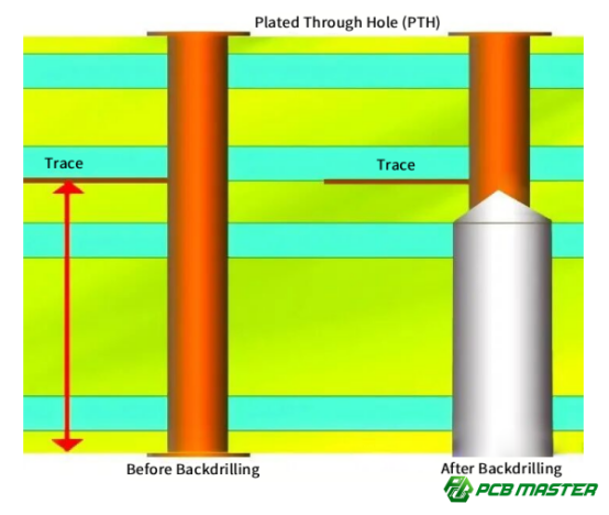
A server PCB backdrill stub (via stub) is the unused portion of a plated through via that extends beyond the signal’s active layer, and it must be precisely controlled because it introduces impedance discontinuities, resonance, and signal reflections that directly degrade high-speed signal integrity.
Stub Definition and Formation Causes
A PCB stub is the unused copper section of a via that does not carry signal and remains after layer transition, and it must be controlled because it behaves like a signal disturbance point in high-speed channels.
In a multilayer server PCB (12–24 layers commonly) , a signal via (Plated Through Hole, PTH) often connects only part of the stack-up. For example, a signal may travel from L1 to L6, but the via barrel continues down to the bottom layers. The unused portion below the last active layer becomes the via stub .
This happens because manufacturing drills straight through the board to form the via. Even if the signal only needs part of the structure, the remaining copper barrel cannot be automatically removed without a secondary process.
After layer transition, this unused copper acts like a “dead-end” transmission path. In high-speed PCB design, this is a major issue because it introduces electrical discontinuities.
Backdrilling is used to solve this problem. A controlled drill removes the unused via section from the back side of the PCB, leaving only the required via length. For example, in a 16-layer AI server board, backdrilling may remove 0.3–0.8 mm of extra via length depending on the target layer.
How Stub Affects High-Speed Signal Integrity
Stub degrades signal integrity by creating resonance, impedance mismatch, reflection, and electromagnetic radiation.
At high data rates like 25Gbps or above, even a small via stub can behave like a resonant structure. A key issue is quarter-wave resonance , where the stub length matches a fraction of the signal wavelength. This creates a strong reflection point, which increases insertion loss and reduces signal energy reaching the receiver.
Another effect is parasitic capacitance and inductance . Each 1 mm of stub can add roughly 0.5–1 pF capacitance and 0.3–0.5 nH inductance. This disturbs the designed impedance, for example dropping a 100Ω differential channel to 70–80Ω locally, causing signal mismatch.
In real systems, this shows up as:
- Eye diagram closure in high-speed links
- Increased jitter in PAM4 signaling
- Reduced channel margin in long PCB traces
Additionally, the stub can act like a small antenna. In a real AI server motherboard, engineers often find EMI test failures caused by poorly controlled via stubs, especially around dense memory and SerDes areas.
Stub Length Tolerance Requirements Across Server Data Rates
As data rates increase, acceptable stub length decreases rapidly, requiring tighter backdrill precision.
In low-speed systems around 10Gbps , a stub length up to about 0.8–1.0 mm is often acceptable because signal wavelength is relatively long, and reflections are manageable.
At 25Gbps , the system enters a sensitive region. Stub length is typically limited to below 0.5 mm. At this level, backdrilling accuracy becomes critical, especially for long backplane or server motherboard traces.
For 56Gbps and 800G optical modules , the requirement becomes much stricter. Stub lengths are often controlled below 0.3 mm. Any deviation can cause measurable degradation in S-parameters, especially S11 reflection performance.
In 112Gbps AI server designs and 1.6T optical interconnects , stub control is extremely tight, typically around 0.1–0.2 mm. At this level, even small mechanical variation in drilling depth can affect signal eye opening.
Looking forward to 224Gbps next-generation interconnects , industry expectation is moving toward near-zero stub designs. This means backdrill processes must achieve ultra-high precision, and in some cases, alternative via structures like blind/buried vias or advanced laminate stackups are used to reduce dependency on mechanical backdrilling.
How is stub length precisely controlled in server PCB backdrilling?
Stub length in server PCB backdrilling is precisely controlled by accurately calculating drilling depth and combining CCD alignment, real-time Z-axis compensation, and multi-level calibration to ensure the backdrill removes the unused via section consistently without damaging the active signal layer.
What factors determine backdrill stub control accuracy?
Stub control accuracy in server PCB backdrilling is mainly determined by board thickness consistency, drill wear, stack-up alignment, and equipment depth precision.
In real server PCB backdrilling processes (14–24 layer AI server boards) , even a small physical variation can change stub length by tens of microns. This is why multiple process factors must be controlled together.
1. Board thickness uniformity and Z-axis compensation
PCB laminates (FR-4 or high-speed materials) often have thickness variation around ±0.05–0.1 mm. If Z-axis depth is not compensated, the backdrill may remove too little or too much copper, leaving an inconsistent stub. High-end fabs use pre-measured board thickness data to adjust drilling depth for each panel.
2. Drill bit wear impact on depth stability
As a drill bit processes thousands of holes (typically 1500–3000 holes per bit), wear changes its cutting behavior. This can cause depth drift in backdrilling. For example, worn tools may leave a 0.05–0.1 mm residual stub compared to a fresh tool. Diamond-coated or carbide drills are commonly used for stability.
3. Stack-up matching and reference layer alignment
If the PCB stack-up is asymmetric or poorly referenced, the backdrill target layer position becomes uncertain. This directly affects stub control. In AI server designs, symmetric stack-ups are preferred to ensure stable drilling reference points.
4. Machine depth control limitation
Even high-end CNC drilling machines have mechanical tolerances (±20–30 μm). Without calibration, this tolerance can accumulate and create inconsistent stub lengths across panels.
How is backdrill depth calculated?
Backdrill depth is calculated by subtracting the target signal layer position from total board thickness and then adding a controlled compensation value.
A standard PCB backdrill depth calculation formula is:
Backdrill Depth = Total PCB Thickness − Distance from Backdrill Entry Side to Target Layer + Compensation Value
This ensures the drill stops just above the active signal layer, leaving minimal or zero stub.
Parameter explanation:
- Total PCB thickness: measured full board thickness after lamination
- Target layer distance: distance from backdrill side to signal termination layer
- Compensation value: correction for tool wear, resin shrinkage, and machine tolerance
Example: In a 16-layer server PCB, if the signal ends at L6 and total thickness is 1.6 mm, engineers may calculate a backdrill depth of around 1.25 mm with a +0.02 mm compensation margin to ensure full stub removal.
Compensation principle: Manufacturers typically use empirical data from process capability (Cp/Cpk) to adjust compensation. High-volume AI server PCB production often updates compensation weekly based on real measurement feedback.
How does CCD vision positioning improve backdrilling accuracy?
CCD vision systems improve backdrill accuracy by visually aligning PCB position and correcting mechanical misplacement in real time.
A CCD-based drilling system uses high-resolution cameras to detect fiducial marks on the PCB. These marks act as reference points for X-Y positioning. The system can achieve alignment accuracy of around ±5 μm in advanced setups.
Dynamic correction of PCB deformation and loading error: During manufacturing, PCB panels may bend or shift slightly due to heat or handling. CCD vision detects these deviations and adjusts drilling coordinates before machining begins, ensuring the backdrill hits the exact target via location.
Real example in AI server PCB production: In large 600 mm server boards, even a 0.1 mm misalignment can cause partial stub removal failure. CCD correction ensures consistent backdrill centering across all vias, especially in high-density SerDes routing areas.
How does a three-level calibration system ensure stable depth control?
A three-level calibration system ensures consistent backdrill depth by combining machine setup calibration, per-board adjustment, and in-process inspection.
1. Startup test drilling calibration:
At the beginning of production, a standard calibration board is drilled to verify Z-axis accuracy. If deviation exceeds ±0.02 mm, the machine is recalibrated before mass production begins.
2. Per-panel thickness compensation
Each PCB panel is measured using laser thickness sensors before drilling. The system automatically adjusts backdrill depth to compensate for small thickness variations between panels.
3. Mid-process sampling and stop rules
After every 50 boards, 1–2 samples are checked for depth accuracy. If stub deviation exceeds ±0.03 mm, production is stopped immediately for adjustment. This prevents systematic batch failure.
In high-volume server PCB manufacturing , this system is critical because even small drift can affect hundreds of boards in a single production run.
Where is electrical depth control technology used in ultra-high-speed PCB applications?
Electrical depth control is used in ultra-high-speed PCB backdrilling where mechanical accuracy alone cannot guarantee near-zero stub requirements.
Working principle: Instead of relying only on mechanical depth, electrical detection monitors conductivity changes between layers. When the drill reaches a target copper boundary, electrical feedback signals the machine to stop automatically.
Difference from mechanical control:
- Mechanical control relies on Z-axis distance only
- Electrical control uses real-time signal feedback from copper layers
- This reduces dependency on material variation and tool wear
Application in 112G+ systems:
In 112Gbps AI servers and 1.6T optical interconnect boards , signal margins are extremely tight. Even a 0.05 mm stub variation can affect eye diagrams and increase bit error rate. Electrical depth control helps achieve near-zero stub consistency, which is critical for these high-speed SerDes channels.
In advanced production lines, electrical control is often combined with CCD positioning and multi-stage calibration to achieve full-process precision control for next-generation server PCB backdrilling.
What design rules must be followed for stub control in server PCB backdrilling?
Stub control in server PCB backdrilling must follow design rules that ensure proper backdrill hole sizing, maintain a safe clearance (typically 8–10 mil) above the target signal layer, and use a well-controlled, symmetrical stack-up with tight thickness tolerances to guarantee accurate and repeatable stub removal without affecting active signal integrity.
Backdrill hole size design principles
Backdrill hole size must be carefully matched to the original via size and adjusted with a controlled clearance to ensure effective stub removal without damaging signal layers.
In server PCB backdrilling design (especially 112G+ AI server boards) , the backdrill hole diameter is usually larger than the original plated through via (PTH). This is necessary to fully remove the unused via stub without touching the active signal portion.
1. Relationship between backdrill and original via size
A standard design rule is that the backdrill diameter is typically 0.15 mm to 0.30 mm larger than the original via drill size. For example, if a via is 0.30 mm, the backdrill may be 0.45–0.60 mm depending on stack-up and tolerance.
2. Common diameter increment guidelines
- Low-speed boards: +0.10–0.15 mm clearance
- Server boards (25G–56G): +0.15–0.25 mm clearance
- High-speed AI boards (112G+): +0.20–0.30 mm clearance
The goal is to ensure complete stub removal while avoiding copper damage to adjacent layers or signal pads. In real manufacturing cases, insufficient clearance often leads to partial stub remaining, which causes impedance discontinuity.
How to set backdrill safety margin correctly?
Backdrill safety margin is set by leaving a controlled distance above the target signal layer, typically 8–10 mil, to avoid cutting into active traces while ensuring full stub removal.
1. Safety distance above target layer principle
In PCB backdrill stub length control design, engineers must ensure the drill stops slightly above the active signal layer. This prevents accidental damage to the functional via section or nearby routing traces.
A typical safety rule is:
- Leave a buffer zone between backdrill endpoint and target layer copper
- This buffer absorbs mechanical tolerance and material variation
2. 8–10 mil design margin practice
In most server PCB backdrilling design rules, an 8–10 mil (0.20–0.25 mm) margin is widely used. For example:
- If target layer position varies slightly due to lamination tolerance
- The safety margin ensures no accidental over-drilling
In high-speed AI server boards, tighter margins may be used, but only with advanced CCD and electrical depth control systems.
A real production example: in a 24-layer AI motherboard, engineers set a 9 mil margin to balance yield and signal integrity, avoiding both residual stub and over-drill risk.
What are the key stack-up design considerations for high-speed server PCBs?
High-speed server PCB stack-up must be symmetrical, tightly controlled in thickness, and designed with manufacturing tolerance windows to ensure stable backdrill performance.
1. Importance of symmetrical stack-up design
A symmetrical PCB stack-up reduces board warping during lamination and reflow processes. Warping can shift via positions, which directly affects backdrill accuracy and increases stub variation.
In AI server designs, symmetry also helps maintain consistent impedance across differential pairs used in SerDes channels.
2. Core material and PP thickness tolerance control
In server PCB stack-up design for backdrilling, core (core board) and PP (prepreg) thickness variations must be tightly controlled, typically within ±0.05 mm. If thickness varies too much, backdrill depth calibration becomes unstable, leaving inconsistent via stubs.
For example, a 16-layer board may use multiple PP layers; even a small 0.03 mm deviation per layer can accumulate into a significant backdrill error.
3. Leaving manufacturing compensation windows
Designers must include a manufacturing tolerance window for backdrilling. This means:
- Avoid placing high-speed vias too close to critical layer boundaries
- Reserve space for depth compensation and drill tolerance
- Allow small adjustment ranges in CAD design rules
In real production, this “ design-for-manufacturing (DFM) buffer” significantly improves yield in 112G and 224G server PCB backdrill processes , where precision requirements are extremely strict.
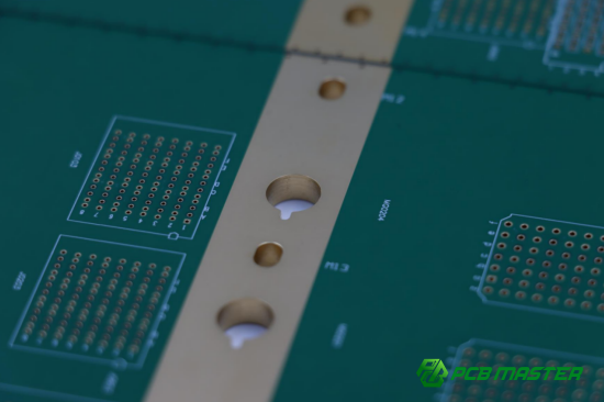
How is stub length measured after server PCB backdrilling?
Stub length after server PCB backdrilling is measured either by direct cross-section microscopy (microsection) that physically reveals and measures the remaining via barrel, or indirectly through TDR and VNA testing by analyzing signal reflection and impedance changes to infer the residual stub length.
How does cross-section (microsection) testing measure stub length?
Cross-section testing measures stub length by physically cutting the PCB and directly observing and measuring the remaining via stub under a microscope.
In server PCB backdrill stub length verification , microsection (also called metallographic analysis) is the most accurate method. It is widely used in AI server PCB manufacturing and high-speed backdrill process validation.
1. Testing process and steps
The PCB sample is first cut through the center of the backdrilled via. It is then embedded in resin, polished layer by layer, and finally observed under a metallographic microscope. This allows engineers to clearly see the via barrel, signal layer, and remaining stub.
2. Direct measurement method of stub height
Once the cross-section is exposed, the stub length is measured vertically from the last active signal layer to the end of the remaining copper barrel. This is a direct physical measurement of via stub length in PCB backdrilling.
3. ±5μm high-precision advantage
Microsection testing can achieve measurement accuracy up to ±5 micrometers. This is critical for 112G and 224G high-speed PCB backdrilling, where even very small stub variations can affect impedance and eye diagram performance.
4. Use cases: first article inspection and failure analysis
This method is mainly used for:
- First article verification in PCB manufacturing
- Process capability (Cp/Cpk) evaluation
- Root cause analysis of signal integrity failures in server PCB designs
For example, if a 56G server board shows unexpected insertion loss, microsection analysis can confirm whether excessive stub length is the root cause.
How does TDR testing enable non-destructive stub detection?
TDR (Time Domain Reflectometry) detects stub length by sending a fast electrical pulse into the trace and analyzing signal reflections caused by impedance changes.
In non-destructive PCB backdrill stub testing , TDR is widely used for server PCB signal integrity validation because it does not damage the board.
1. TDR reflection measurement principle
A fast rise-time pulse is injected into the transmission line. When the signal hits a discontinuity such as a via stub, part of the signal is reflected back. This reflection pattern reveals the location and severity of the stub.
2. Time delay to stub length conversion
By measuring the time difference between transmitted and reflected signals, engineers can calculate distance using signal propagation speed in PCB dielectric material. This allows indirect estimation of via stub length in backdrilled PCBs.
3. Online testing and impedance validation advantages
TDR is suitable for production environments because it enables:
- 100% non-destructive inspection
- Fast inline testing of server PCB batches
- Real-time impedance discontinuity detection
For example, in a high-volume AI server PCB line, TDR can quickly flag boards with abnormal stub-induced reflections without cutting samples.
4. IPC testing standard reference
TDR testing is commonly aligned with standards such as IPC-TM-650 2.5.5.7, which defines time-domain impedance measurement methods used in high-speed PCB characterization.
How does a vector network analyzer evaluate via stub impact?
A vector network analyzer evaluates stub impact by measuring high-frequency S-parameters (S11 and S21) to detect signal reflection and transmission loss caused by residual stubs.
In high-speed server PCB backdrill analysis , a Vector Network Analyzer (VNA) is used to evaluate how via stubs affect overall channel performance.
1. Meaning of S11 and S21 parameters
- S11 (return loss): measures how much signal is reflected back due to impedance mismatch
- S21 (insertion loss): measures how much signal passes through the channel
A poor backdrill with long stubs typically increases S11 and worsens S21 performance.
2. Using reflection patterns to identify stub condition
In real measurements, a well-controlled backdrill shows smooth impedance response. If a stub remains, the VNA trace shows abnormal resonance peaks or dips at specific frequencies, indicating via stub resonance in PCB backdrilling structures.
3. Stub critical threshold and performance inflection point
In many high-speed PCB designs (25G–112G SerDes channels), there is a clear performance cliff:
- Small stub variation → minor impact
- Around a critical length (often ~0.1–0.3 mm) → sharp degradation in S11 and eye diagram closure
This “inflection point” is why precise backdrill control is essential in AI server PCB design.
4. High-speed signal integrity validation use case
VNA testing is commonly used in:
- 112G PAM4 channel validation
- 1.6T optical module interconnect testing
- High-end server motherboard compliance testing
For example, in a 112G AI server link, engineers use VNA S-parameter scans to confirm that backdrilled vias do not introduce resonance within the Nyquist frequency band, ensuring stable high-speed data transmission.
How should different stub length testing methods be selected?
Different stub length testing methods in server PCB backdrilling should be selected based on the production stage and objective—using microsection for accurate physical validation, TDR for fast non-destructive process control, and VNA for high-frequency signal integrity evaluation in advanced 112G/224G applications.
Comparison of microsection, TDR, and network analyzer methods
The choice of stub length testing method depends on whether you need physical accuracy, production efficiency, or high-frequency signal validation in server PCB backdrilling.
In PCB backdrill stub testing for server and AI boards , three main methods are commonly used: microsection (cross-section), TDR testing, and vector network analysis (VNA) . Each method serves a different purpose in the manufacturing and validation flow.
| Test Method | Microsection (Cross-section) | TDR Testing | Network Analyzer (VNA) |
| Detection Type | Destructive | Non-destructive | Non-destructive |
| Measurement Target | Actual physical stub length | Signal reflection position | High-frequency S-parameters |
| Accuracy Level | Very high (direct measurement) | High (calculated distance) | Indirect evaluation |
| Mass Production Use | No | Yes | Yes |
| Main Use Case | First article inspection | Inline sampling & process control | Signal integrity validation |
Key interpretation:
- Microsection = “see the real structure”
- TDR = “see time-domain reflection behavior”
- VNA = “see frequency-domain signal impact”
For high-speed server PCB backdrilling (112G+ applications) , engineers often use all three in combination rather than relying on a single method.
How to choose testing methods for different application scenarios?
Stub testing methods should be selected based on production stage: development needs physical validation, production needs speed, and high-speed design needs electrical performance confirmation.
1. Process development stage
At this stage, engineers focus on understanding the real backdrill behavior. Microsection (cross-section analysis) is the preferred method because it directly shows the physical stub structure. It is commonly used to optimize drilling depth, verify compensation values, and study via behavior in new server PCB stack-ups.
2. First article approval stage (FAI)
In this stage, both accuracy and repeatability are important. A combination of microsection + TDR testing is often used. Microsection confirms actual stub length, while TDR ensures the electrical response matches expectations. For example, in a 24-layer AI server board, first article inspection may require ±5 μm physical confirmation plus impedance verification.
3. Mass production stage
In high-volume server PCB backdrilling production, efficiency is critical. Therefore, TDR testing becomes the main method because it is fast, non-destructive, and suitable for inline sampling. Microsection is only used periodically for audit purposes.
4. 112G / 224G ultra-high-speed validation stage
For next-generation AI server and 1.6T interconnect systems, electrical performance becomes the dominant factor. Here, vector network analysis (VNA) is essential to evaluate S11 and S21 behavior. Engineers use VNA to detect resonance caused by residual stubs that may not be visible in time-domain testing.
For example, in a 112G PAM4 channel, a small stub variation may not change physical measurements significantly, but VNA can clearly show eye diagram degradation risk through frequency-domain anomalies.
Summary logic for selection:
- Need physical truth → Microsection
- Need fast process control → TDR
- Need high-frequency performance validation → VNA
- Need full confidence in 112G+ designs → Combine all three methods
Why is 0.1mm stub length control becoming the new standard in AI server PCBs?
0.1mm stub length control is becoming the new standard in AI server PCBs because ultra-high-speed signals like 112G/224G PAM4 have extremely tight noise and timing margins, making even tiny via stubs a major source of reflection, impedance discontinuity, and eye diagram degradation that can compromise link reliability.
Why are 112G PAM4 signals highly sensitive to via stubs?
112G PAM4 signals are highly sensitive to via stubs because they operate with extremely tight noise margins and high frequency components, making even very small stub variations cause serious signal distortion.
In 112G PAM4 AI server PCB backdrilling applications , signal integrity margins are extremely small. The signal uses multiple amplitude levels (PAM4), which means even minor noise or reflection can cause bit errors.
1. Reduced noise margin challenge
At 112G speeds, the voltage difference between signal levels is very small. A tiny via stub can introduce impedance mismatch, which increases noise and reduces the available margin for correct signal detection. In real AI server motherboard designs, this can directly reduce link stability in SerDes channels.
2. Eye diagram closure and BER risk
A via stub behaves like a small resonator. At high frequency, it reflects part of the signal back into the channel. This causes eye diagram closure, which means the signal becomes harder to distinguish between logic levels. As a result, the bit error rate (BER) increases, especially in long backplane or high-density routing environments.
For example, in a 112G switch board, engineers observed that reducing stub length from 0.3 mm to 0.1 mm significantly improved eye opening and reduced error bursts under heavy traffic.
How is stub control evolving from 25G to 224G?
As data rates increase from 25G to 224G, acceptable stub length rapidly decreases, pushing manufacturing from sub-millimeter control to near micro-scale precision.
1. Shrinking stub tolerance window
At 25G, PCB designs may tolerate up to ~0.5 mm stub length with manageable signal degradation. However, at 56G and 112G, this tolerance drops sharply to around 0.2 mm. In 224G next-generation interconnects, the target is approaching ~0.1 mm or even lower.
This trend is driven by higher frequency content and shorter signal wavelengths, which make via stubs act more like resonant structures rather than simple parasitic elements.
2. Manufacturing precision moving to micron level
To meet 112G/224G server PCB backdrilling requirements, manufacturers must control drilling depth, stack-up variation, and tool wear at micron-level precision. This includes advanced CCD alignment, real-time Z-axis compensation, and tighter material thickness control.
For example, leading AI server PCB fabs now routinely measure thickness variation in the ±5–10 μm range to maintain consistent stub control across large panels.
Why is backdrilling shifting from an optional process to a critical capability?
Backdrilling is becoming a critical capability because AI servers require extremely stable high-speed interconnects, and PCB manufacturers must ensure near-zero stub performance to meet system-level reliability requirements.
1. AI server demand for high-reliability interconnects
Modern AI systems rely on massive data movement between GPUs, CPUs, and high-speed memory. Any signal degradation caused by via stubs can lead to retransmissions, latency increase, or even link failure. Therefore, PCB backdrilling stub control is no longer optional—it is essential for stable system operation.
In real hyperscale data centers, even small signal integrity improvements can translate into significant performance gains across thousands of compute nodes.
2. Backdrilling as a key competitive capability for PCB manufacturers
In the high-end PCB industry, especially for 112G/224G AI server boards, backdrilling precision is now a key differentiator. Manufacturers compete based on:
- Minimum achievable stub length (e.g., 0.1 mm control capability)
- Depth accuracy stability across mass production
- Yield rate consistency in high-layer-count boards (20+ layers)
For example, PCB suppliers capable of stable sub-0.1 mm stub control are often selected for advanced AI accelerator and 1.6T optical module platforms.
In this context, server PCB backdrilling technology has evolved from a manufacturing step into a core engineering competency that directly defines product competitiveness.
Conclusion
Via stubs have become one of the most critical factors affecting signal integrity in high-speed server PCB backdrilling, particularly as data rates push into the 112G and 224G PAM4 era. At these speeds, even a very small residual stub can introduce noticeable impedance discontinuity, signal reflection, and eye diagram closure, which ultimately impacts link stability and system reliability.
To manage this risk effectively, stub length control is no longer a single-process task, but a tightly coordinated system that connects design, manufacturing, and inspection. In practice, this requires careful stack-up planning, precise backdrill depth control, and continuous compensation based on real production feedback to keep variation within a tightly controlled window.
On the manufacturing side, technologies such as CCD visual alignment, three-stage depth calibration, and electrical depth control are now widely used to push backdrilling accuracy into the sub-0.1 mm range. At the same time, verification must be multi-layered: microsection provides physical truth, TDR supports fast process monitoring, and vector network analysis confirms high-frequency signal behavior.
As AI servers and 1.6T optical interconnect systems continue to evolve, this level of precision is no longer optional but expected. Consistently controlling residual stub length at or below 0.1 mm has effectively become a new benchmark for advanced server PCB manufacturing.
In this context, experienced PCB and PCBA providers like PCBMASTER play a practical role by integrating design support, process control, and testing capability into a unified workflow, helping ensure stable and repeatable performance in next-generation high-speed applications.
FAQs
Why do server PCBs require backdrilling, while standard PCBs usually do not?
Server PCBs require backdrilling because high-speed signals (25G–224G) are highly sensitive to via stubs, which cause reflection, resonance, and signal loss. Standard PCBs operate at much lower frequencies, where these effects are negligible, so stub removal is not necessary.
What stub length is acceptable for 112G PAM4 applications?
For 112G PAM4 server PCB applications, stub length typically must be controlled within 0.1–0.2 mm , with advanced designs targeting ≤0.1 mm to ensure stable eye diagrams, low bit error rate (BER), and controlled impedance.
Can TDR testing fully replace microsection (cross-section) analysis?
No, TDR testing cannot fully replace microsection analysis. TDR is excellent for fast, non-destructive process monitoring, but microsection provides direct physical measurement of actual stub length and is still required for first article inspection and failure analysis.
How is backdrill depth compensation value determined?
Backdrill depth compensation is determined based on real manufacturing data, including PCB thickness variation, tool wear, and machine tolerance. In practice, it is calibrated using process capability data (Cp/Cpk) and verified through periodic microsection and TDR feedback loops.
Will future 224Gbps high-speed PCBs require “zero stub” control?
Yes, 224Gbps PCB designs are moving toward near “zero-stub” conditions because signal wavelengths are extremely short and even 0.1 mm stubs can significantly degrade performance. In many cases, designers will rely on advanced backdrilling, blind/buried vias, or alternative stack-up structures to effectively eliminate usable stub impact.
About the Author

Carol Luo
PCB Design EngineerI'm Carol, a PCB Engineer at PCBMASTER with experience in PCB design and manufacturing engineering since 2018. I focus on translating engineering requirements into reliable PCB solutions, with expertise in stack-up design, material selection, and design-for-manufacturing (DFM). I share practical engineering insights from real-world PCB design and production experience.
Visit Carol Luo's Profile