


What Is GND (Ground) in Electronics? Meaning, Types, and PCB Design Guide
GND (Ground), often referred to as a ground wire, is one of the most fundamental concepts in electronics, PCB design, and electrical engineering. It serves as the common reference point for voltage measurements and provides a return path for electrical current within a circuit. Whether in consumer electronics, industrial control systems, automotive electronics, or communication equipment, proper grounding is essential for circuit stability, signal integrity, electromagnetic compatibility (EMC), and user safety.
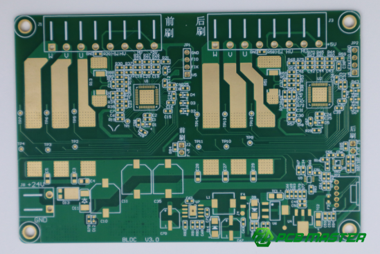
For engineers and manufacturers, understanding the role of GND in PCB and PCBA design helps reduce noise, improve performance, and ensure reliable operation. As a leading PCB and PCBA manufacturer, PCBMASTER assists customers in implementing optimized grounding strategies through advanced PCB fabrication, engineering review services, and high-quality assembly processes.
Understanding the Meaning of GND in Electronics
GND stands for Ground, a designated reference point in an electrical or electronic circuit from which voltages are measured.
In most electronic systems, ground serves two primary functions:
1. Voltage Reference Point
1. All voltages within a circuit are measured relative to ground.
2. A 5V signal means the signal is 5 volts higher than the ground reference.
2. Current Return Path
1. Electric current must complete a loop.
2. Ground provides a path for current to return to the power source.
Without a properly designed ground connection, circuits may become unstable, noisy, or completely nonfunctional.
Simple Example
Consider a basic LED circuit:
· Power Supply: +5V
· LED
· Resistor
· Ground (GND)
Current flows from the positive terminal, through the resistor and LED, and returns through the ground connection. The circuit only works because the current has a complete path.
Why Is Ground Important in PCB Design?
Grounding affects nearly every aspect of PCB performance.
Signal Integrity
Modern electronic devices often contain high-speed digital signals. Poor grounding can introduce:
· Signal distortion
· Data errors
· Timing issues
· Crosstalk
A well-designed ground system helps maintain clean signal transmission.
Noise Reduction
Ground planes reduce electromagnetic interference (EMI) and electrical noise by providing a low-impedance return path.
Safety Protection
In power electronics and industrial systems, grounding can help prevent dangerous voltage buildup and protect users from electrical shock.
Thermal Management
Large copper ground planes can also assist with heat dissipation, improving overall system reliability.
Types of Ground in Electronics
Not all grounds are identical. Different applications use different grounding schemes.
Earth Ground
Earth ground is physically connected to the earth through grounding rods or building electrical systems.
Common applications include:
· Industrial equipment
· Power distribution systems
· Household electrical installations
Chassis Ground
Chassis ground connects electronic circuits to a metal enclosure.
Benefits include:
· EMI shielding
· Improved safety
· Enhanced system stability
Signal Ground
Signal ground serves as the reference point for analog and digital signals.
Examples include:
· Microcontrollers
· Sensors
· Communication modules
Power Ground
Power ground carries higher currents associated with power delivery circuits.
Common applications:
· Motor drivers
· DC-DC converters
· Power supplies
Analog Ground vs. Digital Ground
In mixed-signal systems, engineers often separate analog and digital grounds to reduce interference.
| Parameter | Analog Ground (AGND) | Typical Applications |
| Primary Function | Sensitive analog signals | High-speed digital circuits |
| Noise Sensitivity | Very high | Moderate |
| Typical Devices | ADCs, DACs, amplifiers | MCUs, processors, FPGAs |
| Routing Strategy | Isolated and controlled | Wider return paths |
| Connection Method | Single-point connection | Integrated system ground |
Proper grounding becomes increasingly important in applications such as:
· Medical devices
· Automotive electronics
· Industrial automation
· RF communication equipment
Ground Plane in PCB Design
A ground plane is a continuous copper layer dedicated to GND.
It is one of the most effective PCB design techniques for improving electrical performance.
Advantages of Ground Planes
· Lower impedance return paths
· Reduced EMI emissions
· Improved signal integrity
· Better thermal distribution
· Simplified routing
Ground Plane Example
For a 4-layer PCB:
| Layer | Function |
| Top Layer | Signal |
| Inner Layer 1 | Ground Plane |
| Inner Layer 2 | Power Plane |
| Bottom Layer | Signal |
This structure is widely used in high-speed digital and communication products.
Common Grounding Mistakes
Design Issue Potential Consequence Broken ground plane Increased EMI and signal noise Long return current paths Signal integrity degradation Multiple uncontrolled ground connections Ground loops Narrow ground traces Voltage drops and heating Mixing noisy and sensitive circuits Analog signal corruption
| Design Issue | Potential Consequence |
| Broken ground plane | Increased EMI and signal noise |
| Long return current paths | Signal integrity degradation |
| Multiple uncontrolled ground connections | Ground loops |
| Narrow ground traces | Voltage drops and heating |
| Mixing noisy and sensitive circuits | Analog signal corruption |
Ground Loops: A Common Engineering Challenge
A ground loop occurs when multiple ground paths exist between two points.
This can cause:
· Noise injection
· Audio hum
· Measurement inaccuracies
· Communication failures
Ground loops are particularly problematic in:
· Audio equipment
· Industrial control systems
· Medical electronics
· Sensor networks
Engineers typically minimize ground loops through careful PCB layout and single-point grounding strategies.
Best Practices for PCB Ground Design
Use a Solid Ground Plane
Avoid fragmented or heavily split ground layers whenever possible.
Keep Return Paths Short
Current naturally follows the path of least impedance. Ensure signals have nearby ground return paths.
Separate Sensitive Circuits
Keep analog, digital, RF, and power circuits properly partitioned.
Use Multiple Ground Vias
Ground stitching vias help maintain low impedance and improve EMI performance.
Review Manufacturability Early
Grounding performance can be affected by stack-up design, copper balancing, via structures, and manufacturing tolerances.
This is why professional engineering review before fabrication is highly recommended.
PCBMASTER's Grounding Expertise in Advanced PCB Manufacturing
As a professional PCB and PCBA manufacturer serving customers worldwide, PCBMASTER supports grounding-critical applications across automotive electronics, industrial control systems, communications equipment, medical devices, and consumer electronics.
Leveraging its 80,000㎡ manufacturing facility, PCBMASTER provides:
· High-frequency PCB manufacturing
· HDI PCB production
· Rigid-Flex PCB fabrication
· Flexible PCB (FPC) solutions
· Advanced multilayer PCB stack-up design support
Quality Assurance for Ground-Critical Designs
PCBMASTER maintains rigorous quality standards through:
· IATF 16949 certification
· ISO 9001 quality management system
· UL certification
· RoHS compliance
· Advanced AOI inspection
· Three-stage quality inspection processes
· 100% electrical testing before shipment
Engineering Support
PCBMASTER's engineering team provides:
· Free design file review
· Ground plane optimization recommendations
· DFM (Design for Manufacturability) analysis
· Stack-up consultation
· Signal integrity guidance
By identifying potential grounding issues before production, PCBMASTER helps customers reduce redesign cycles, improve product reliability, and accelerate time-to-market.
Future Trends in Ground Design
As electronic devices continue to evolve toward:
· Higher frequencies
· Faster data rates
· Greater integration density
· More compact form factors
Grounding design is becoming increasingly critical.
Emerging technologies such as:
· 5G infrastructure
· AI hardware
· Automotive ADAS systems
· Industrial IoT
· High-speed networking equipment
require advanced PCB grounding techniques to achieve optimal performance and electromagnetic compatibility.
Manufacturers and design teams that prioritize grounding early in the development process will gain significant advantages in product reliability, certification success, and long-term system performance.
Conclusion
GND (Ground) is far more than a simple wire connection—it is the foundation of every electronic circuit. Acting as both a voltage reference and current return path, proper grounding directly impacts signal quality, EMI performance, safety, and overall product reliability.
Whether designing a simple embedded device or a complex multilayer HDI PCB, implementing effective grounding strategies is essential for success. Through advanced manufacturing capabilities, engineering expertise, and internationally certified quality systems, PCBMASTER helps customers transform grounding best practices into high-performance, production-ready electronic products.
Tags: #PCB #PCBA #SMT #GroundWire #GND #PCBDesign #HDIPCB #SignalIntegrity #EMI #ElectronicsManufacturing #PCBMASTER #IndustryInsights

