


High-Frequency PCBs The Invisible Bridges of the Digital World—Decoding the Technology Behind a $100 Billion Market Over the Next Decade
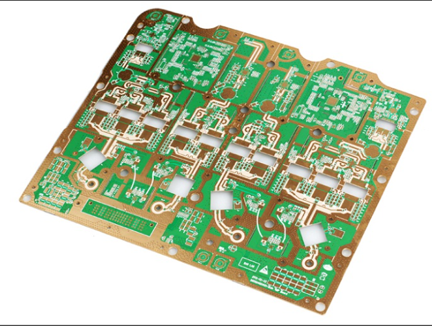
At an autonomous vehicle testing site in Beijing engineer Wang Tao installs a palm-sized circuit board into a rooftop radar. This black substrate, etched with wave-like gold traces, processes millimeter-wave signals at 24 billion cycles per second—a core component ensuring cars can detect pedestrians in heavy rain. Once confined to military applications, high-frequency PCBs are now the invisible backbone driving trillion-dollar industries like 5G, satellite internet, and autonomous driving.
I. 5G/6G Communications: The "Golden Track" for High-Frequency PCBs
According to Prismane Consulting, the global market for high-frequency PCBs in 5G base stations will surpass $8.2 billion by 2027, with a CAGR of 19.3%. Key breakthroughs include:
2.Material Innovation: Huawei verified that modified PTFE (Dk=2.17±0.02, Df=0.0009@110GHz) boosts 64T64R Massive MIMO antenna efficiency by 23%.
3.3D Integration: Ericsson’s 6G trials achieved 1.2 Tbps/mm² transmission density using embedded coaxial structures (0.05mm inner diameter).
Thermal Management: ZTE’s graphene composite substrate (thermal conductivity: 8.3 W/mK) reduced base station power consumption by 15%.
A 2024 test at a Jiangsu smart factory showed 5.5G micro base stations with new high-frequency PCBs achieved a 1.2 km coverage radius (vs. 800m traditionally) and latency as low as 0.8 ms.
II. Automotive Electronics: The "Neural Evolution" of Millimeter-Wave Radar

Tesla’s latest autonomous system uses 18 high-frequency PCBs, with specs leaping exponentially:
Parameter | 2020 Solution | 2025 Target |
Frequency | 77 GHz | 140 GHz |
Angular Resolution | 1.5° | 0.3° |
Detection Range | 250 m | 500 m |
Temp Tolerance | -40°C to 105°C | -55°C to 150°C |
Key advancements:
1.Heterogeneous Integration: Infineon bonded GaN amplifiers directly to PCBs, cutting signal loss by 42%.
2.Dynamic Impedance Compensation: Bosch’s AI algorithm adjusts impedance for 1,200 traces in real time (<±0.8Ω variation).
3.Nanoscale Surface Treatment: Molecular self-assembled monolayers (SAMs) extend gold finger durability to 500,000 cycles.
III. Satellite Internet: Extreme Challenges in Space
1.High-frequency PCBs in SpaceX Starlink satellites endure:
①Thermal Cycling: -180°C to +130°C
②Radiation: 300 krad total ionizing dose
③Microgravity Stress: Structural deformation up to 0.3 GPa
2.Lockheed Martin’s solutions:
①Ultra-Low CTE Composites: Silicon carbide-reinforced LCP (CTE=2.1 ppm/°C)
②Atomic Layer Deposition: 5nm alumina coating reduces EMI leakage by 35 dB
③Biomimetic Cooling: Honeycomb copper pillars lower thermal resistance to 0.08°C/W
2023 tests showed these PCBs degraded just 1.2% over 5 years in orbit—far exceeding NASA standards.
IV. Medical Electronics: The Battle for Microvolt Signal Integrity

1.In the seventh-gen da Vinci surgical system, high-frequency PCBs face:
①Noise Suppression: Crosstalk < -70 dB at 0.5mm spacing
②Impedance Precision: ±0.5% tolerance (vs. ±10% for standard PCBs)
2.Medtronic’s breakthroughs:
①EM Funneling: Gradual microstrip lines absorb 90% of stray radiation.
②Biocompatible Coating: 0.1μm parylene layer passes ISO 10993-5 cytotoxicity tests.
③LTCC Integration: 120 embedded capacitors in 8-layer boards slash response time to 0.1 ns.
Clinical data shows 50-micron precision in neurointerventional surgeries—an industry record.
V. Three Technical Barriers in a $100 Billion Market
1.Material Limitations:
①PTFE’s CTE (50 ppm/°C) triples copper’s, risking solder fatigue.
②Toray’s carbon nanotube-enhanced PTFE (CTE=18 ppm/°C) is now in Huawei’s 6G prototypes.
2.Manufacturing Precision:
Metric | 2023 Level | 2030 Target |
Line Width Tolerance | ±3 μm | ±0.8 μm |
Dielectric Uniformity | ±5% | ±1.5% |
Via Position Accuracy | ±12 μm | ±3 μm |
TSMC’s electron-beam lithography (EBL) trials achieve stable 0.6 μm line widths.
3.Testing Revolution:
①256-channel near-field scanners detect 0.005 mm² EMI hotspots.
②Multi-axis vibration-humidity chambers simulate typhoons and sandstorms.

