PCBMASTER Presents A Comprehensive Guide to PCBA Design Engineering – In-Depth Analysis from Principles to Practice
Author: Jack Wang
I. Core Value and Industry Status of PCBA Design
PCBA (Printed Circuit Board Assembly) design is the core stage of electronic product development, directly impacting product performance, reliability, and production costs. According to the IPC-2221B standard, proper PCBA design can improve product yield by over 30% while reducing post-production maintenance costs by 15%–25%. The global Electronics Manufacturing Services (EMS) market reached $587 billion in 2023, where PCBA design quality directly affects over 65% of customer satisfaction.

1. Material Selection and Layer Stackup Architecture
①Base Material Selection: FR-4 (Tg≥170°C) is suitable for most consumer electronics, while Rogers RO4350B (εr=3.48) is recommended for high-frequency applications.
②Layer Stackup Design: A 6-layer board structure (Top-GND-Signal-Power-Signal-Bottom) meets 80% of mid-to-high-speed circuit requirements.
③Copper Thickness Selection: 1 oz (35μm) for outer layers and 0.5 oz (17.5μm) for inner layers provide the optimal cost-performance ratio.
2. Signal Integrity Design
①Impedance Control: Differential line impedance tolerance must be within ±10% (refer to IPC-2141A).
②Equal-Length Routing: DDR4 trace length deviation should be ≤50 mil (1.27 mm).
③Via Design: Laser microvias with 0.2mm/0.45mm (hole diameter/pad size) are recommended for 8-layer boards.
3. Thermal Management Solutions
①Thermal Copper Areas: Power devices require a heat dissipation area of ≥4 cm²/W.
②Thermal Interface Materials: Combine thermal conductive silicone (3.5 W/m·K) with phase-change materials (5.2 W/m·K).
③Temperature Monitoring: Implement a 3-tier temperature alert system (60°C/85°C/105°C).
II.Common Design Pitfalls and Solutions
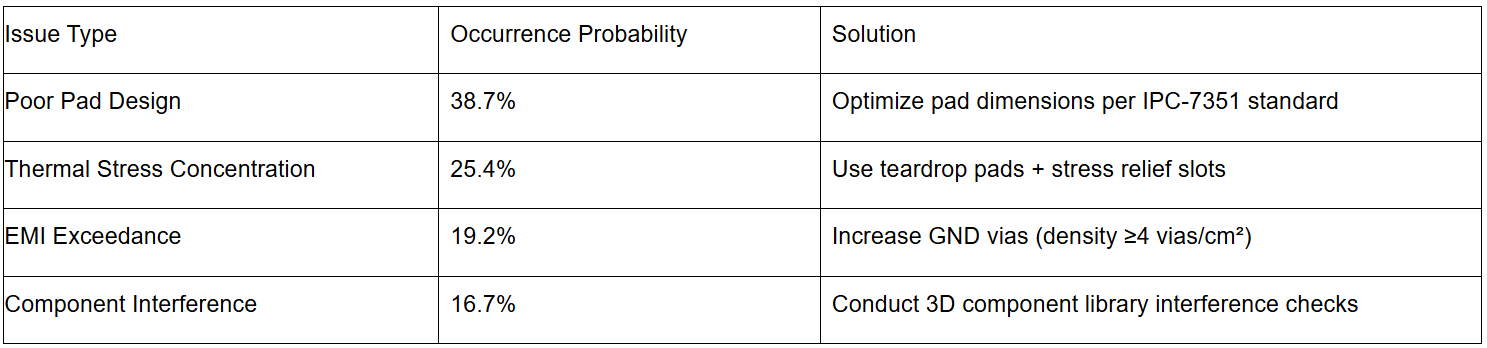
(Data Source: 2023 International Conference on Electronic Failure Analysis)
III. Advanced Design Tools and Engineering Practices
1.DFM Inspection Systems: Valor NPI software detects over 98% of process risks automatically.
2. Simulation Platforms: HFSS + HyperLynx co-simulation achieves <5% error.
3.Prototyping Workflow: Execute 3 design iterations (schematic validation → pre-production validation → mass production validation).
IV.Industry Trend Predictions
1.High-Density Interconnect (HDI): mSAP technology enables 20μm line width/spacing.
2.Embedded Components: Passive component embedding saves 40% board space.
3.Intelligent Design: AI-driven AutoRouter algorithms boost efficiency by 300%.
Conclusion
Outstanding PCBA design requires balancing three critical factors: electrical performance, manufacturability, and cost control. By adopting standardized design processes (aligned with IPC-2221 standards), implementing rigorous design reviews (≥3-tier sign-off), and leveraging modern EDA tools, product development cycles can be shortened by over 40%. With the rise of 5G and AIoT technologies, PCBA design is evolving from traditional circuit layout to system-level collaborative design, demanding engineers to master both foundational circuit knowledge and cross-domain design expertise.
Author: Jack Wang