


Engineering Guide for Ceramic-Based Aluminum Nitride PCBs From Material Properties to High-Reliability Design

Ⅰ. Core Material Properties of Ceramic-Based PCBs
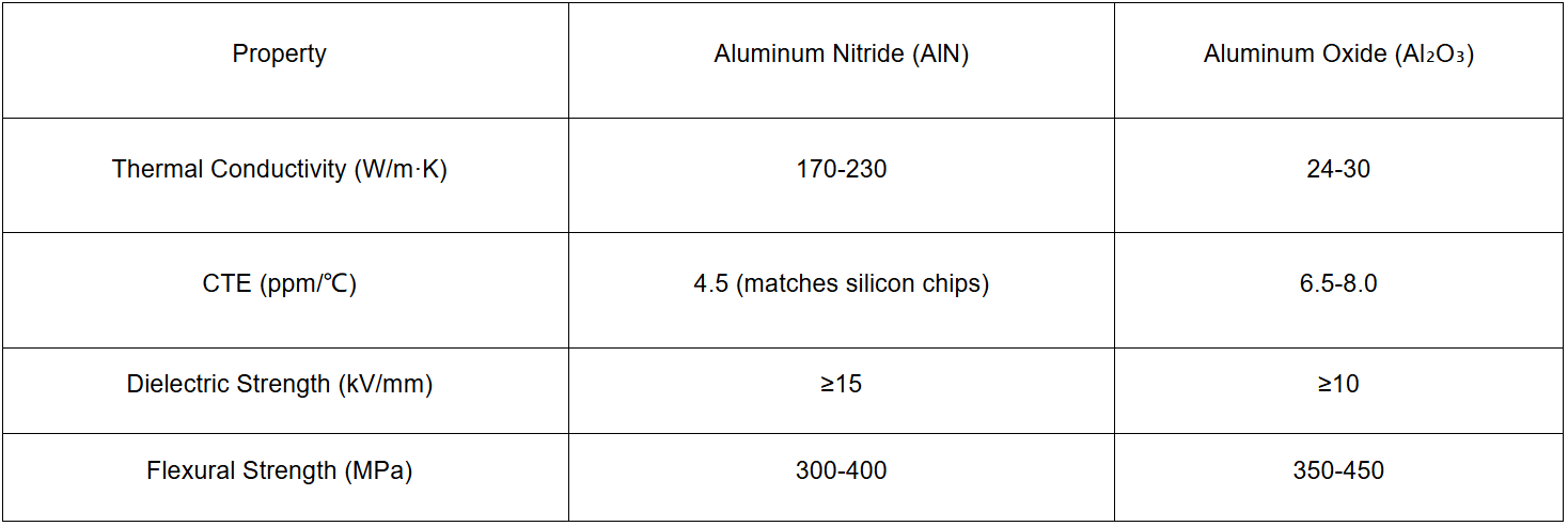
Ceramic-based PCBs have become the preferred solution for high-power electronics due to their exceptional thermal conductivity and mechanical stability. Aluminum Nitride (AlN) and Aluminum Oxide (Al₂O₃) are the most widely used ceramic substrates. Key parameter comparisons are as follows:
Technical Notes:
①AlN’s thermal conductivity is 7× higher than Al₂O₃, making it ideal for high heat flux scenarios (>50W/cm², e.g., LiDAR, IGBT modules).
②Ceramic-based aluminum oxide PCBs remain cost-effective (priced at 1/3–1/2 of AlN) for medium-low power applications like LED lighting and automotive sensors.
Ⅱ. Four Key Design Challenges & Solutions for AlN PCBs
2.1 Microvia Metallization Optimization
AlN surface activation requires specialized processes:
①Two-step etching after laser drilling (NaOH pretreatment + H₃PO₄ micro-etching).
②Adhesion strength ≥8N/mm (ASTM D4541). Sputtered TiW/electroless Ni delivers optimal results.
2.2 Thermal Stress Matching Design
For operating temperatures (-55°C to 150°C):
①Power layer copper thickness ≥200μm (+40% current capacity).
②Signal layer copper thickness: 35μm (reduces thermal stress concentration).
2.3 High-Frequency Signal Integrity Control
At >10GHz frequencies:
①Dielectric loss tangent (tanδ) ≤0.001 (AlN measures 0.0008 at 10GHz).
②Ground via spacing < λ/10 (<0.3mm for millimeter-wave bands) in coplanar waveguide designs.
2.4 Hermetic Packaging Compatibility
For aerospace applications (MIL-STD-883K compliance):
①Pad surface roughness Ra ≤0.5μm (prevents helium leak test failures).
②Gold plating thickness ≥1.27μm (withstands >500hrs salt spray testing).
Ⅲ. Application-Specific Selection Guidelines
3.1 Mandatory Use Cases for AlN PCBs:
①SiC power modules (junction temperature >175°C).
②Phased array radar TR components (heat flux >80W/cm²).
③UV laser driver circuits (CTE matching >95%).
3.2 Preferred Scenarios for Ceramic-Based Aluminum Oxide PCBs:
①Automotive oxygen sensors (operating temperature <200°C).
②Industrial PLC boards (cost-sensitive mass production).
③Medical monitoring devices (ISO 13485 certification required).
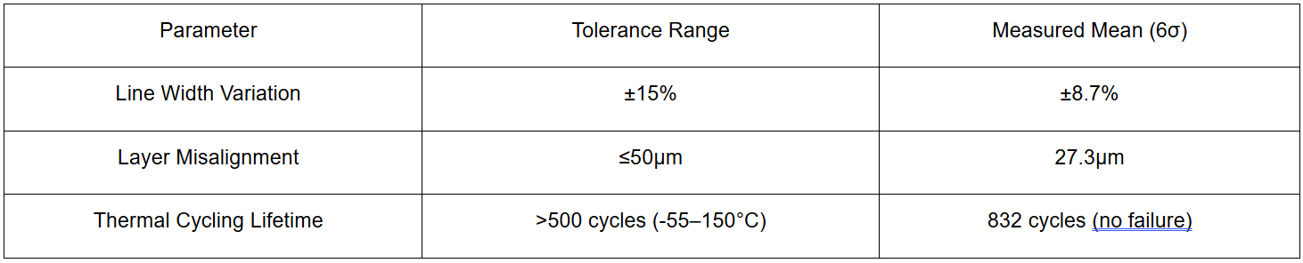
Ⅳ.Process Windows Revealed by Empirical Data
Statistical analysis of 200+ AlN PCB samples (per IPC-6012D):
Conclusion
Ceramic-based aluminum nitride PCBs are redefining high-power electronics design, while ceramic-based aluminum oxide PCBs maintain dominance in mid-range markets due to mature manufacturing processes. Engineers must evaluate thermal requirements, budgets, and reliability needs to select the optimal ceramic substrate.
(Data sources: Kyocera Technical White Paper, IPC-6012D, NASA MSFC-2020 Thermal Management Report)
Aluminum Nitride Ceramic-Based PCB The Core Driver of Next-Generation High-Power Electronics

