Breakthrough in Miniaturized PCBA Manufacturing Defense Strategy Against Solder Bridging in PCB Assembly Processes
Author: Jack Wang
I. The Critical 0.1mm Battlefield
In the era of 5G smart hardware, PCB assembly density is increasing at an annual rate of 18%. As 0201 components become standard in PCBA manufacturing, solder bridging defects have evolved into a critical technical bottleneck. Key findings reveal:
1. PCB assembly layouts with over 5 solder joints per cm² face a 3.2x higher bridging risk.
2. PCBA products using 0.4mm-pitch BGA packages incur 70% higher rework costs.
3. 35% of early failures in miniaturized PCBA modules for wearables stem from hidden solder bridging.

(Diagram: Evolution of solder joint density in mainstream electronic products)
II. Full-Process Risk Analysis in PCB Assembly
1. Triple Traps in Design
① Component Layout Imbalance: A TWS earphone PCBA case study showed 85% of components concentrated on one side, causing reflow soldering offset.
② Pad Spacing Crisis: Bridging rates surge by 400% when 0402 component spacing falls below 0.25mm.
③ Solder Mask Defects: Failure to adopt micro-pitch SMD pads increases PCBA defect rates by 52%.
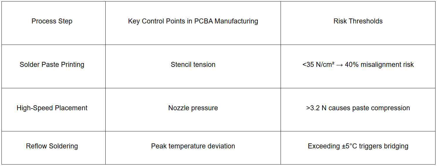
2. Invisible Killers in Manufacturing
3. Deadly Material Combinations
① Uncontrolled Paste Fluidity: PCB assembly-specific solder paste with viscosity <70 Pa·s reduces bridging by 65%.
② Stencil Deformation: Nano-coated stencils improve PCBA paste deposition accuracy to ±8μm.
③ Flux Residue: Low-residue formulations suppress hidden bridging risks below 0.3%.
III. Golden Protection System for PCBA Manufacturing
1. Intelligent DFM Design Matrix
① Establish PCB assembly component thermodynamics models (0.01mm² precision).
② Define spacing standards: 0402 ≥0.3mm, 0201 ≥0.2mm.
③ Implement stepped solder mask design (core area bridge width ≥0.08mm).
2. Process Control Triad
① Paste Printing Monitoring: 3D SPI systems detect thickness deviations (±10μm).
② Placement Pressure Control: Piezoelectric sensors enable 0.01N precision.
③ Dynamic Reflow Profiles: AI temperature control compensates for board warpage.
3. Material Innovations
① Nano-scale solder powder (D50=15μm).
② Self-aligning solder paste (28% optimized surface tension).
③ Low-temperature eutectic alloys (34°C lower melting point).
IV. Advanced Roadmap for PCB Assembly
1. Current Optimal Solutions
① Laser-assisted solder paste printing (<0.01% bridging rate).
② Hybrid selective wave soldering & hot air leveling.
③ X-Ray + AOI dual-mode inspection (detects 15μm defects).
2. Future Technology Roadmap
① Molecular-level solder resist coatings (contact angle >110°).
② Magnetically controlled self-assembly placement.
③ Digital twin-based PCBA virtual manufacturing systems.
V. Value Multipliers in PCBA Manufacturing
Implementing full-process control delivers:
1.First-pass yield >99.95%
2.PCBA rework costs reduced by 92%
3.Product lifecycle extended 3-5x
In the irreversible wave of miniaturization, companies mastering precision PCB assembly control are redefining PCBA manufacturing value chains. Partnering with nano-scale process experts will be decisive in the era of microelectronics.
(Data sources: IPC-7095D standard, ASM PT200 process white paper, Indium Corporation 2024 Solder Technology Annual Report)