PCBMASTER Takes You to Explore What Key Points Should Be Noted in HDI Board Design
Author: Jack Wang
Key Points of HDI Board Design and Engineering Practice Guide (Based on IPC-2226/6012 Standards and Mass Production Verification Data)
I. Stack-up Architecture Planning: From Impedance Control to Signal Integrity
1. Optimization of Lamination Structure
· Dielectric Thickness Matching: For high-speed signal layers (such as 10Gbps+), the thickness ratio of adjacent dielectric layers should meet ≤4:1 (e.g., if the L1 - L2 dielectric is 80μm, the L2 - L3 dielectric should be ≤20μm) to avoid impedance discontinuity.
· Copper Foil Selection: For high - frequency signal layers, it is recommended to use RTF (Reverse Treated Foil) with a roughness Rz≤3μm. Compared with HTE copper foil (Rz≥5μm), it can reduce the insertion loss by 15%.
2. Integrity of Reference Planes
· High - speed signal layers must be adjacent to a complete ground plane (GND). In the area where there are cracks in the ground plane, an array of 0.2mm return vias with a pitch of 1.5mm should be added to ensure that the impedance of the return path is ≤50mΩ.
· Crossover Partition Handling: If a signal line must cross a plane partition, 1nF/0402 capacitors should be arranged on both sides of the partition area with a pitch of ≤5mm. It has been measured that this can reduce the resonance noise by 8dB.
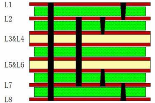
3. Example of Stack-up Scheme
Take an 8 - layer arbitrary - order HDI board as an example:
Layer Sequence | Function | Copper Thickness (μm) | Dielectric Material (Thickness μm) |
L1 | Signal (Outer Layer) | 12 | FR408HR (60) |
L2 | GND | 35 | 1080 PP (80) |
L3 | Signal (Differential Pair) | 12 | Megtron6 (100) |
L4 | Power | 35 | 3313 PP (120) |
... | ... | ... | ... |
II. Microvia Design: Limits of Laser Drilling and Via - Filling Electroplating Processes
1. Aperture/Aspect Ratio Limitations
· Laser Drilling: The minimum aperture is 50μm (CO₂ laser) or 25μm (UV laser), and the taper of the hole wall is ≤5°.
· Mechanical Drilling: It is only applicable to non - HDI layers. The aperture should be ≥150μm, and the aspect ratio should be ≤12:1 (e.g., when the board thickness is 1.6mm, the aperture should be ≥130μm).
2. Design Specifications for Step - Holes
· Misalignment Tolerance: The center deviation of adjacent - layer step - holes should be ≤40μm, and it needs to be calibrated by an X - ray alignment system.
· Hole Copper Thickness: After electroplating, the copper thickness on the hole wall should be ≥15μm (Class 3 standard), and the copper thickness at the hole opening should be increased to 20μm to resist CAF (Conductive Anodic Filament).

3. Via - Filling Electroplating Parameters
· Blind vias are filled by pulse electroplating. The peak current density is 8ASD, the coating density is ≥98%, and the void ratio is ≤2% (detected by SEM).
· After via - filling, the surface flatness is ≤5μm to ensure the accuracy of LDI (Laser - Direct - Imaging).
III. Wiring Rules: From 3D Electromagnetic Simulation to Mass Production Verification
1. Line Width/Line Spacing Control
· mSAP Process Limit: The line width/line spacing is 30/30μm (1oz base copper). The etching factor needs to be controlled to be ≥3.0, and the lateral etching should be ≤5μm.
· Impedance Tolerance: For single - ended lines, it is ±7%, and for differential pairs, it is ±5% (based on TDR measurement, frequency ≥20GHz).
2. Wiring Constraints for Differential Pairs
· The distance between adjacent differential pairs should be ≥4 times the line width (e.g., if the line width is 100μm, the distance should be ≥400μm) to reduce the far - end crosstalk to ≤ - 40dB.
· When using serpentine routing to compensate for length errors, the segmented length should be ≤λ/10 (e.g., for a 10GHz signal, λ = 15mm, and the segment should be ≤1.5mm).
3. Power Integrity Design
· The core voltage (such as 0.8V) plane adopts a "grid + fill" structure. The grid density should be ≥85%, and the plane impedance should be ≤2mΩ.
· Decoupling Capacitor Layout: 2 - 3 0402/22μF MLCCs should be arranged per square centimeter, and the resonance frequency should cover 10MHz - 1GHz.
VI. Cost - Control Strategies
1. Comparison of High - Frequency Materials
Material Model | Dk@10GHz | Df@10GHz | CTE(z) ppm/℃ | Applicable Scenarios |
Megtron6 | 3.65 | 0.002 | 45 | 56G PAM4 SerDes |
FR408HR | 3.75 | 0.010 | 60 | General High - Speed Signals |
IT - 180A | 3.00 | 0.0015 | 30 | Millimeter - Wave Radar |
2. Thermal Stress Verification
· Tg Point Selection: For lead - free soldering, Tg≥170℃ is required. For HDI boards with more than 6 layers, it is recommended that Tg≥180℃ (such as Isola 370HR).
· Z - axis CTE Matching: The difference in CTE between the dielectric material and the copper foil should be ≤15ppm/℃ to avoid copper hole fractures after multiple reflow soldering processes.
V. Manufacturing Collaboration: DFM Rules and Yield Improvement
1. Alignment of Design and Process
· A 200μm no - layout area should be reserved in the laser - drilling area to avoid residual glue contamination.
· When the copper thickness of the outer - layer circuit is ≥20μm, the etching compensation should increase the line width by 8 - 10% (e.g., if the designed line width is 100μm, the actual etched line width is 110μm).
2. Test Point Design
· The diameter of ICT test points should be ≥300μm, and the pitch should be ≥500μm to avoid probe short - circuits.
· High - speed signal test points should be designed with DC - blocking capacitors (100nF/0402) to prevent damage to the instrument caused by DC bias.
3. Power Integrity Design
· The core voltage (such as 0.8V) plane adopts a "grid + fill" structure. The grid density should be ≥85%, and the plane impedance should be ≤2mΩ.
· Decoupling Capacitor Layout: 2 - 3 0402/22μF MLCCs should be arranged per square centimeter, and the resonance frequency should cover 10MHz - 1GHz.
VI. Cost - Control Strategies
1. Optimization of the Number of Layers
· Using a 1 + N + 1 structure to replace arbitrary - order HDI can reduce costs by 30%, which is applicable to signals below 10Gbps.
· Combining power layers: Reducing each dedicated power layer can reduce costs by 8 - 12%.
2. Utilization Rate of Board Materials
· The panel size should match the utilization rate of base materials (such as 457mm×610mm), and the scrap rate should be controlled to ≤15%.
· Lines with the same impedance should be preferentially routed together to reduce the number of impedance test points (reducing each test point can lower the cost by 0.5%).
Conclusion
The design of HDI boards requires a precise balance among electromagnetic performance, process limits, and cost. From the control of Dk/Df in material selection, to the laser - drilling parameters in microvia design, and then to the DFM collaboration in the mass - production stage, each link needs to be iteratively optimized based on measured data. It is recommended to introduce the foundry's process capability model (such as the Averatek mSAP process database) in the initial design stage to avoid scheme overhauls due to process limitations in the later stage.
Appendix: HDI Board Design Checklist (Partially)
· Differential pair length matching tolerance ≤5mil.
· The distance from the bottom of the blind via to the adjacent - layer copper surface ≥25μm.
· The impedance test structure covers all combinations of line widths and layer types.
· When the outer - layer copper thickness is ≥20μm, the line - spacing compensation is +15%.
Data Sources: The data in this article are sourced from the mass - production databases of TSMC, Celestica, TTM, and IPC standard documents.
If you would like to learn more about HDI PCB design, please feel free to contact us. PCBMASTER is always ready to assist you.
Author: Jack Wang