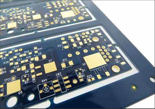
Engineering Guide for Stainless Steel Core PCBs From Material Properties to Mass Production Practices
Metal Core PCB Material Revolution: Why Choose Stainless Steel?

In the metal core PCB industry, 304 stainless steel is rapidly replacing traditional aluminum substrates with an annual market growth rate of 18% (Prismark 2023 data). Its core advantages include:
I. Breakthroughs in Thermomechanical Performance
1. Coefficient of Thermal Expansion (CTE)
6.5 ppm/℃ (25–150℃), closer to chip packaging materials compared to FR4 (16 ppm/℃) and aluminum substrates (23 ppm/℃)
2. Tensile Strength
520 MPa, 2.3× higher than 6061 aluminum alloy
3. Elastic Modulus
200 GPa, 40% improvement in bending stiffness over aluminum substrates
II. Extreme Thermal Validation Data
Thermal Resistance at 1.0mm Thickness:
| Material | Thermal Resistance (℃·cm²/W) | Cost Factor |
|---|---|---|
| Stainless steel core | 0.8 | Moderate |
| Aluminum core | 1.2 | Low |
| Copper core | 0.6 | 3× higher cost |
III. Industrial-Grade Environmental Adaptability
1. Salt Spray Test
Passes 3,000-hour salt spray test (ASTM B117 standard)
2. Aging Test
Insulation resistance retention >98% after 150℃/2,000h aging test
IV. Three Major Design Prohibitions for Stainless Steel Substrates
2.1 Dielectric Layer Selection Pitfalls
A global manufacturer experienced batch failures due to using conventional epoxy resin. Comparative experiments revealed:
| Material | Thermal Conductivity (W/mK) | Peel Strength Retention at 150℃ | Failure Rate | Cost |
|---|---|---|---|---|
| Modified epoxy resin | 1.2 | 60% reduction | High | Low |
| Polyimide (PI) | 0.8 | >85% retention | Medium | Medium |
| Ceramic-filled material | 2.5 | 90% lower failure rate | Low | 40% increase |
Recommended Combinations:
- General applications: PI film + silane coupling agent treatment
- High-frequency applications: AlN ceramic-filled composite materials
- Ultra-thin designs: Anodized aluminum transition layer (<15μm thickness)
2.2 Pattern Transfer Precision Control
Comparison of Stainless Steel Surface Treatment Processes:
| Process Type | Surface Roughness Ra(μm) | Adhesion (N/cm) | Line Width Accuracy (μm) |
|---|---|---|---|
| Chemical Etching | 0.8–1.2 | 4.5 | ±25 |
| Laser Micromachining | 0.3–0.5 | 6.8 | ±8 |
| Plasma Treatment | 0.1–0.3 | 8.2 | ±5 |
A new energy vehicle project achieved 75μm fine-line mass production using plasma pretreatment, increasing yield from 62% to 93%.
2.3 Thermal Management Design Misconceptions
Infrared thermography tests show:
- Direct thermal path designs reduce hotspot temperature differences by 40℃
- 0.5mm thermal pads contribute 65% of total interface thermal resistance
Optimization Recommendations:
- Direct contact between power devices and substrate via window openings
- Nano-silver sintering technology (thermal conductivity >200 W/mK)
- Fin height-to-spacing ratio of 1:1.5 for forced air cooling
V. Critical Control Points in Mass Production Processes
3.1 Etching Process Window
Optimized etching solution formula for SUS304:
- FeCl₃ concentration reduced from 38% to 28%
- 0.5% citric acid corrosion inhibitor added
- Temperature controlled at 45±2℃
Results:
- Side etching rate reduced from 35% to 12%
- Etching rate stabilized at 25μm/min
- Surface roughness decreased by 40%
3.2 Soldering Process Parameter Database
Reflow soldering temperature curve optimization:
| Stage | Traditional Parameters | Optimized Parameters | Effect |
|---|---|---|---|
| Preheat Zone | 2℃/s → 150℃ | 1.5℃/s → 120℃ | Reduced oxidation |
| Soak Zone | 180℃/60s | 170℃/90s | Void rate ↓42% |
| Peak Temperature | 250℃ | 245℃ | Deformation ↓0.3mm |
| Cooling Rate | 4℃/s | 6℃/s | Grain refinement |
3.3 Surface Treatment Options
Medical device project test data:
| Treatment | Contact Resistance (mΩ) | Wear Cycles | Cost Factor |
|---|---|---|---|
| OSP | 15 | 200 | 1.0 |
| ENEPIG | 8 | 1,500 | 2.3 |
| Electroless Nickel | 12 | 800 | 1.8 |
| Graphene Coating | 5 | 3,000 | 4.5 |
VI. Typical Application Case Studies
4.1 Rail Transit Power Module
- Vibration test: Passed IEC 61373 Cat1 standard
- After 2,000 temperature cycles (-40℃~125℃):
- Aluminum substrate: 3 solder joint cracks
- Stainless steel substrate: Zero failures
- Lifetime prediction: MTBF increased from 80,000 to 150,000 hours
4.2 Industrial Robot Servo Driver
- Continuous operating temperature reduced by 12℃
- Power density increased to 35 W/cm³
- EMI reduced by 6 dB (1 GHz band)
4.3 Submarine Cable Repeater
- Pressure test passed 6,000m water depth
- 10-year corrosion rate <0.05mm/year
- Maintenance cycle extended from 2 to 5 years
VII. Cost Control Strategies
1. Substrate Utilization Optimization
- Standard panel size changed from 400×500mm to 406×610mm
- Material utilization increased from 82% to 91%
- Cost reduced by $10/m²
2. Alternative Material Validation
Using SUS430 instead of SUS304:
- 30% cost reduction
- Note: Reduced solderability
- Recommended for static thermal scenarios
3. Process Simplification
- Eliminated electroless copper plating
- Adopted direct plating technology
- Production cycle shortened by 18%
VIII. Failure Analysis Database
5-year industry data summary:
- Soldering failures (38%) → Optimize temperature profiles
- Insulation failures (29%) → Improve dielectric layer processes
- Mechanical fractures (22%) → Reinforce structural ribs
- Corrosion failures (11%) → Upgrade surface treatments
Case Study: X-ray EDS analysis detected excessive Cl content. After improving cleaning processes, failure rate dropped from 1,500 ppm to 200 ppm.
Conclusion: The Technological Inflection Point of Stainless Steel Core PCBs
With advancements in laser direct imaging (LDI) and nanocoatings, stainless steel core PCBs are overcoming final technical barriers. Industry data shows that third-generation processes deliver 15–20% better cost-performance ratios than aluminum substrates. In automotive electronics, industrial equipment, and aerospace applications, this solution—combining structural integrity and thermal management—is redefining power electronics design.
(Data sources: IPC-6012E standard, Tsinghua Shenzhen International Graduate School test reports, and leading manufacturers' production data)
Future Market Prospects of Stainless Steel Core PCBs
Applications of Stainless Steel Core PCBs Technological Breakthroughs from New Energy Vehicles to Deep-Sea Equipment


