


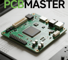
Introduction to Surface Mount Technology (SMT) Knowledge
Surface Mount Technology (SMT), originally created and developed in the 1980s and initially called planar mounting, revolutionized PCB assembly by allowing components to be mounted directly onto the surface of printed circuit boards. This breakthrough created new opportunities for miniaturization and automation in electronics manufacturing, transforming the electronics manufacturing world. Advancements in SMT and related technologies continue to shape the industry, creating more efficient and higher-quality production systems that impact daily life.
Today, the relentless trend towards miniaturization, weight reduction, and enhanced performance in electronic products provides powerful momentum for the widespread application of SMT. This technology enables the integration of more components within limited space, significantly increases assembly speed, and perfectly aligns with automated production demands. SMT allows for the use of multiple layers in PCB construction, enabling complex circuit assemblies and improved signal integrity. Consequently, from everyday consumer electronics and precision medical devices to complex automotive electronic systems, SMT has become an indispensable core process. Most modern electronics are manufactured using SMT, offering advantages in cost, automation, and miniaturization.
This article will delve into the definition, core value, significant advantages, standard SMT PCB assembly processes, common soldering methods, and the fundamental differences between SMT and traditional THT. It will also highlight how specialized companies like PCBMASTER deliver highly reliable SMT process solutions.
Core Concept of Surface Mount Technology (SMT)
SMT, an abbreviation for Surface Mount Technology, centers on mounting electronic components (known as Surface Mount Devices, SMDs) directly onto the solder pads of a Printed Circuit Board (PCB) and soldering them in place. These surface mount components are mounted directly onto the PCB surface, without the need for through-holes, enabling higher component density and more compact assemblies. This stands in stark contrast to Through-Hole Technology (THT), also known as through hole mounting, which requires inserting component leads into PCB through-holes for soldering. The THT process is a reliable method for applications needing strong mechanical bonds and is better suited for vibration conditions, such as aerospace or military devices, and for external devices that require frequent manual handling or replacement. The THT process involves more manual intervention, is relatively less efficient, and more prone to errors. SMT, however, achieves a high degree of automation, effectively reducing production time and costs while improving product consistency and efficiency. It’s noteworthy that in practice, a single PCB can utilize both SMT and THT techniques, as certain specific components (like high-power DC-DC converters, transformers, etc.) may not be suitable for surface mounting or when SMT as the sole attachment method is limiting in high-stress applications.
Common Surface Mount Device (SMD) Package Types
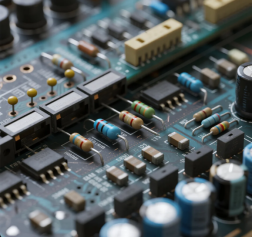
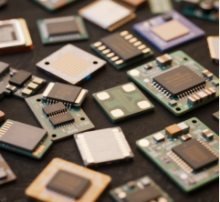
Components used in SMT are collectively called Surface Mount Devices (SMDs), encompassing resistors, capacitors, inductors, diodes, integrated circuits (ICs), and many others. These SMDs come in diverse physical size specifications, known as different “packages.” Surface mount components are designed for automated assembly and are essential in modern electronics manufacturing.
Numerous standard SMD package types exist for resistors, capacitors, inductors, diodes, and ICs. Below are some of the most commonly applied types:
Resistor, Capacitor, Inductor, Diode Packages:
·0201 (0.6×0.3 mm): Miniature size, primarily used in Radio Frequency (RF) circuits.
·0402 (1.0×0.5 mm): Commonly found in sensors and consumer electronics.
·0603 (1.5×0.8 mm): Widely used in audio equipment and defense applications.
·0805 (2.0×1.3 mm): Extensively applied in industrial and military sectors.
·1206 (3.0×1.5 mm): Frequently used in power electronics.
Integrated Circuit (IC) Packages:
·DIP (Dual In-line Package): Easy for manual handling, commonly used in prototyping.
·SOP (Small Outline Package): Compact structure, a mainstream choice for consumer electronics.
·TSOP (Thin Small Outline Package): Small volume, mainly used for memory (e.g., RAM).
·QFP (Quad Flat Package): Beneficial for increasing PCB wiring density.
·QFN (Quad Flat No-leads Package): Widely used in smartphones and industrial electronics.
·BGA (Ball Grid Array Package): The preferred package for microprocessors and controllers.
·LQFP (Low-profile Quad Flat Package): Highly prevalent in IC manufacturing.
·TQFP (Thin Quad Flat Package): Suitable for small devices with space constraints.
·SOIC (Small Outline Integrated Circuit): Commonly used for LDO regulators, heat sinks, etc.
·TSSOP (Thin Shrink Small Outline Package): A common package in consumer electronics.
·PBGA (Plastic Ball Grid Array): A type of BGA, mainly used in microprocessor development.
SMD packages are designed to contain all the components needed for a device in a compact form, supporting the miniaturization and integration of electronic assemblies.
Application Scenarios of SMT Technology
Modern electronic devices like smartphones and laptops continue evolving towards greater intelligence and thinner profiles. This trend poses significant challenges for engineers: how to implement more complex functional designs within smaller PCB areas? Surface Mount Technology (SMT), with its exceptional high-density integration capability, provides the “key” to solving this problem, enabling the manufacture of lightweight yet powerful devices. SMT allows manufacturers to create compact and efficient electronic devices by mounting components directly onto the PCB surface, achieving higher component density and improved performance. Consequently, SMT has permeated nearly all electronics manufacturing sectors, including medical devices, aerospace, defense, and consumer electronics.
The core production equipment of SMT – the pick-and-place machine – enables large-scale automated assembly, making it ideal for large Electronics Manufacturing Services (EMS) companies. SME surface mount equipment, such as high-precision pick-and-place machines and reflow ovens, is specialized machinery used for the precise placement and soldering of SMT components. SMT’s comprehensive automated processes deliver extremely high production efficiency and cost-effectiveness. SMT components (SMDs) are tiny, significantly increasing component density per unit area, and also offering advantages for high-frequency circuit performance. For these reasons, mainstream electronics manufacturing widely adopts SMT technology, producing compact, lightweight, high-performance, and reliable products through efficient surface mount PCB assembly. The result is highly integrated electronic assemblies.
Core Advantages of SMT Technology
Compared to THT, SMT possesses a series of significant advantages that have fundamentally transformed PCB manufacturing:
·High-Density Design: SMT components mount directly onto PCB surface pads, eliminating the need for drilled holes. This allows both sides of the PCB to be used for component placement, enabling more complex circuit designs within smaller spaces and achieving higher component density.
·Miniaturized Components: SMDs are significantly smaller than through-hole components, vastly increasing the number of components a PCB can accommodate.
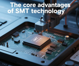
·Efficient Automated Production: Fully automated pick-and-place machines achieve high-speed, high-precision placement of SMDs, particularly suited for high-volume manufacturing. Automation drastically shortens production cycles, improves overall efficiency, and minimizes human errors. Pick-and-place machines and reflow ovens operate to ensure high-speed, accurate placement and soldering of SMT components.
·Superior Electrical Performance: Signal integrity is a core challenge in modern electronic design. The small size and surface mounting of SMT components effectively shorten signal transmission paths. This helps reduce signal crosstalk and minimizes parasitic inductance and capacitance effects, making SMDs ideal for high-frequency circuits. SMT provides lower resistance and lesser lead inductance at connection points, resulting in improved high-frequency performance. Its design leads to a smaller radiation loop area and lower radiated emissions, which is beneficial for electromagnetic compatibility. SMT enables more predictable high frequency performance due to these electrical characteristics.
·Comprehensive Cost-Effectiveness: Economies of scale from automated production lines significantly lower per-unit manufacturing costs.
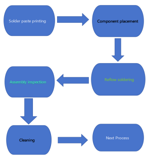
Overview of the Standard SMT Assembly Process
The process of mounting SMDs onto a PCB is called the SMT assembly process, or more formally, SMA surface mount assembly. The manufacturing process primarily consists of the following key steps:
1.Solder Paste Printing: Solder paste, a mixture of solder powder and flux, forms the electrical and mechanical connection between SMDs and PCB pads. The first step involves precisely printing solder paste onto the PCB pads, typically using a metal stencil (solder mask) with cut-out patterns.
2.Component Placement: High-precision automated pick-and-place machines pick up SMDs (resistors, capacitors, ICs, etc.) from feeders and accurately position them onto the PCB pads coated with solder paste.
3.Reflow Soldering: The populated PCB enters a reflow oven. The oven heats the board according to a preset temperature profile (typically including preheat, soak, reflow, and cooling stages), melting the solder paste so it wets the pads and component terminations. Upon cooling, solid, reliable solder joints are formed.
4.Assembly Inspection: After soldering, the PCB undergoes rigorous inspection using Automated Optical Inspection (AOI) or X-ray inspection to identify soldering defects (like bridging, insufficient solder), component misalignment, or missing parts.
5.Cleaning** (Optional):** Depending on the solder paste type and product requirements, the soldered PCB may need cleaning to remove residual flux and other contaminants, ensuring long-term reliability.
Precise measurement and control of units, such as temperature and placement accuracy, are critical in SMT manufacturing to ensure consistent quality throughout the manufacturing process.
Key Soldering Techniques in PCB Assembly
Reflow soldering and wave soldering are the two primary processes in PCB manufacturing.
Wave Soldering:
**·**Primarily used for Through-Hole Components (THT), but can also be used for some SMT components (typically those with short leads).
**·**Process: Insertion -> PCB passes over a wave of molten solder -> Solder contacts solder joints -> Cooling solidification.
**·**Compared to reflow soldering, wave soldering is less efficient, involves more complex process control, and carries a slightly higher risk of defects (like bridging, insufficient solder).
Reflow Soldering:
**·**The standard and preferred soldering process for SMT. Particularly suitable for mass production, offering very high yield and consistency.
**·**Process: Stencil printing solder paste -> Pick-and-place machine mounts SMDs -> Reflow oven soldering (Preheat -> Soak -> Reflow -> Cool).
**·**Its advantages lie in precise control of solder volume per joint, minimal thermal shock, and high soldering quality.
SMT vs THT: Core Differences
Surface Mount Technology (SMT) and Through-Hole Technology (THT) together form the foundation of modern PCB assembly. Although both aim to secure components to the PCB and establish electrical connections, they differ significantly in technical principles, processes, advantages/disadvantages, and application scenarios.
Comparison Dimension | Surface Mount Technology (SMT) | Through-Hole Technology (THT) |
Technical Principle | Components mounted on PCB surface pads | Component leads inserted into PCB through-holes and soldered |
Assembly Process | Highly automated (Core equipment: Pick-and-place, Reflow) | Can be auto-inserted, but soldering (wave) & some steps more manual |
PCB Space Utilization | Very High (Double-sided mounting, miniaturized components) | Lower (Typically single-sided insertion, larger components) |
Component/PCB Bond Strength | Reliable electrical connection, mechanical strength relies mainly on solder joints (weaker than THT) | Very high mechanical strength (leads penetrate PCB & encapsulated by solder) |
Suitable Components | Vast majority of modern components (Res, Cap, IC, BGA, QFN) | High-power/high-heat components (e.g., large transformers, DC-DC modules), connectors |
Initial Investment/Cost | Higher equipment investment (Pick-and-place, Reflow, etc.), but lower per-unit cost at scale | Lower equipment investment, but higher labor costs, less efficient at scale vs SMT |
Rework Difficulty | Higher difficulty (especially micro, multi-pin, bottom-termination ICs like BGA/QFN) | Relatively easier (leads visible and accessible) |
Table: Key Technical Comparison of SMT vs THT
SMT does not offer easy installation compared to through-hole mounting, as it requires more skill and specialized equipment. Relying on SMT as the sole attachment method can be limiting in applications requiring high mechanical strength. Through-hole technology is a reliable method for applications needing strong mechanical bonds and is better suited for vibration conditions, such as aerospace or military devices. Through-hole components are also preferred for external devices that require frequent manual handling or replacement.
Conclusion
Surface Mount Technology (SMT), as a revolutionary breakthrough in electronics manufacturing, has fundamentally reshaped the design and production paradigms of modern electronic products. From its initial applications in the 1980s to its current status as the industry mainstream, SMT, with its core advantages of high-density integration, efficient automation, and superior electrical performance, perfectly aligns with the developmental needs for miniaturized, high-performance electronics. It underpins technological innovation across numerous fields, including consumer electronics, medical devices, and aerospace.
Compared to traditional Through-Hole Technology (THT), SMT demonstrates significant advantages in component density, production efficiency, and cost control. However, the two are not simply replacements; THT remains indispensable in scenarios demanding high power handling or mechanical strength, forming a complementary and coexisting technological landscape.
From standardized processes spanning solder paste application to reflow soldering, to diverse SMD packages and inspection techniques, SMT’s mature system provides the electronics manufacturing industry with flexible and reliable solutions. Looking ahead, as chip packaging miniaturization and process intelligence advance, SMT will continue to push the boundaries of precision and efficiency, remaining the core cornerstone driving continuous innovation in the electronics industry, empowering the creation of thinner, smarter, and more reliable electronic products. SMT has improved the quality of life by enabling faster, more efficient, and environmentally friendly electronic products.
FAQ
Q: Can SMT and THT be used on the same PCB simultaneously?
A:
Yes. In actual production, a single PCB often employs both SMT and THT techniques. This is because certain components (like high-power transformers, connectors) may be better suited for THT due to structural or performance requirements, while the majority can be densely integrated via SMT. Combining both allows for optimized functionality, reliability, and cost.
Q: Why is SMT more suitable for high-frequency circuit design?
A:
SMT components are small and mount directly onto the PCB surface, significantly shortening signal transmission paths. This reduces parasitic inductance, capacitance, and signal crosstalk, which is crucial for signal integrity in high-frequency circuits. In contrast, THT component leads are longer and more prone to introducing additional electrical interference. Therefore, SMT is the preferred solution for high-frequency applications like RF circuits and high-speed data transmission modules. SMT's lower resistance, lesser lead inductance, smaller radiation loop area, and lower radiated emissions all contribute to more predictable high frequency performance.
Q: What are common defects in SMT production? How to avoid them?
A:
Common defects include “tombstoning” (component lifting due to uneven solder melting on its ends), solder bridging (shorts between adjacent joints), and insufficient solder (poor joint formation). Avoidance measures: Optimize pad design (e.g., balance pad size on component ends), precisely control the reflow soldering temperature profile, use high-precision stencils for solder paste printing (ensuring uniform solder volume), and promptly identify issues through AOI/X-ray inspection.
Q: Is SMT more expensive than THT for small-batch production?
A:
Yes. SMT requires significant initial equipment investment (pick-and-place machines, reflow ovens), and setup costs like stencil fabrication and program debugging add extra expense. Therefore, for very small batches, SMT costs can be higher than THT. However, as production volume increases, SMT’s automation efficiency advantage becomes apparent, leading to significantly lower per-unit costs at scale compared to THT.
Q: What is an SMD package? How do different packages impact SMT production?
A:
An SMD package refers to the physical size and structural specifications of a Surface Mount Device (e.g., 0402, QFP, BGA). Impact: Different packages impose varying demands on SMT equipment precision and process parameters. For instance: *** Micro components like 0201 require placement machines with ±15μm or better accuracy. *** Packages with bottom connections like BGA necessitate X-ray inspection to ensure solder joint quality. *** Leadless packages like QFN place higher demands on solder paste printing uniformity.
Q: What are the challenges of working with SMT components?
A:
SMT components often have very small sizes and tight lead spacings, making them difficult to handle, repair, and install. Specialized handling tools, such as tweezers, and sometimes expensive tools are required due to the complexity and miniaturization of small SMT components.
Why PCBMASTER: https://www.pcbmaster.com/why
Join US:https://www.pcbmaster.com/login

