
PCBMASTER Reveals : Avoid These Design Traps to Create High - Reliability PCB and PCBA Products
In the global electronics manufacturing industry, the reliability of PCBs (Printed Circuit Boards) and PCBA (Printed Circuit Board Assembly) directly affects the lifespan and performance of end - products. However, industry data shows that up to 65% of circuit board failures are caused by design defects or process violations. As a technical solution provider with 15 years of experience in the industry, PCBMASTER, based on over 2,000 customer cases, reveals the "high - risk no - go zones" that must be avoided in PCB/PCBA design.
I. Design Phase: These 5 "Fatal Mistakes" Will Directly Lead to Product Failure
1. "Suicidal Wiring" that Violates Line Width/Line Spacing

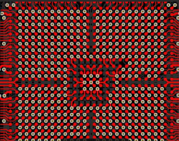
Solution: Use dynamic impedance calculation tools, implement "serpentine equal - length compensation" for high - speed signals, and reserve a 10% line - width redundancy in key areas.
2. The "Invisible Killer" in VIA Design
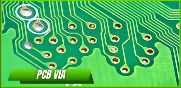
Industry practice: For industrial - grade products, laser drilling (with an accuracy of ±0.025mm) is recommended, combined with the via - filling electroplating process, which can reduce via resistance by 40%.
II. Manufacturing Process: These 3 "Cost - Saving Operations" Are Destroying Product Reliability
1. The "Time Bomb" in Pad Treatment
A certain automotive electronics customer once had a large - scale recall due to improper pad treatment:① Pads without immersion gold treatment, in a high - temperature and high - humidity environment, had a 62% reduction in solder joint strength after 3 months.② For OSP - coated pads using the water - washing process, the wettability decreased by 55% after 5 reflows.
Authoritative data: The ENIG (Electroless Nickel Immersion Gold) process, although it increases costs by 8%, can extend the solder joint life to more than 10 years, and is especially suitable for medical, military, and other scenarios.
2. The "Invisible Defects" in the Solder Mask Layer
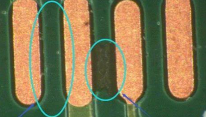
Technical breakthrough: PCBMASTER uses the plasma cleaning technology before solder masking, which can increase the ink adhesion force to the highest 5B level and achieve 100% coverage inspection through Automated Optical Inspection (AOI).
III. Material Selection: The "Slow - Acting Poison" Ignored by 90% of Engineers
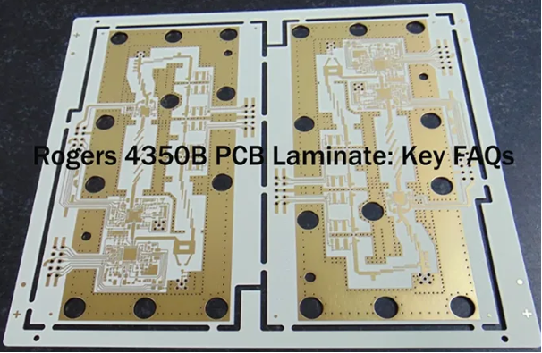
1. The "Temperature Trap" of Substrate Materials
Alternative solution: For high - frequency scenarios, ROGERS 4350B (Dk = 3.48±0.05) is recommended, and for high - temperature environments, Isola 370HR (Tg > 180℃) is used. Although the cost only increases by 15 - 20%, the MTBF (Mean Time Between Failures) is increased by 3 times.
2. The "Chemical Undercurrent" in Surface Treatment
① In a 2022 smartwatch project, due to the out - of - control immersion silver (ImmersionAg) process
② When the silver layer thickness > 0.3μm, the risk of ion migration increased by 7 times.The contact resistance fluctuated by 22% after 6 months of storage.
Process comparison: In scenarios that require long - term storage, electroplated hard gold (with a thickness of 0.05 - 0.1μm) is recommended, combined with the selective immersion gold technology, which can reduce costs by 50%.
IV. Compliance Red Lines: These 2 New Regulations Will Change the Industry Landscape
1.The EU SCIP database requires that, since 2024, PCBA containing > 0.1% lead must declare SVHC substances.
2.The IPC - A - 610H standard update: The allowable deviation for 01005 component placement has been tightened from 30% to 15%.
PCBMASTER has passed the IATF16949 automotive system certification and established a lead - free flexible production line, which can provide customers with "green manufacturing solutions" that comply with RoHS3.0 and REACH.
Author: Jack Wang