PCBMASTER Presents Top 10 Common Errors in PCB Silkscreen Design and Professional Solutions
Author: Jack Wang
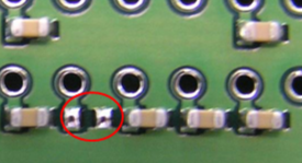
1. Insufficient Pad Clearance (Critical Safe Zone Violation)
Error Description: Silkscreen character edges are placed <0.15mm (6mil) from pads.

Risk Analysis:
Solder mask misalignment may cause solder bridging (incidence rate ~0.3%).
Ink carbonization contaminates solder joints during reflow.
Solutions:
Set a 0.2mm (8mil) safety clearance rule (compatible with 90%+ PCB manufacturers’ processes).
Use Altium Designer’s "Silk to Solder Mask" rule checker.
2. Missing or Ambiguous Polarity Markings
Examples:
Electrolytic capacitors marked only with a "+" symbol, lacking a cathode bar.
LED orientation indicators mismatched with actual package polarity.

Failure Case:
A medical device batch recall due to reversed diode installation (loss: $2.8M).
Design Standards:
Adopt a dual marking system: "△ + pin number" (compliant with IEC 61188).
Add peripheral orientation markers for hidden-pin components (e.g., QFN/BGA).
3. Mismatched Character Size and Line Width
Process Limits:
Minimum line width for conventional silkscreen: 0.15mm (LPI process).
Laser engraving resolution limit: 0.08mm.

Common Errors:
0.5mm-height characters with 0.1mm line width (print breakage rate >40%).
Insufficient background expansion for reverse-font characters.
Golden Ratio Formula:
Character height ≥1.2mm: Line width ≥15% of height.
Character height <1.2mm: Line width ≥0.18mm.
4. Version Information Mismanagement
Industry Lesson:
Mixed old/new components due to unupdated version numbers caused 22-hour production line downtime.

Professional Solutions:
Implement a "VX.Y.Z + date code + checksum" system (e.g., V2.3.1_2405A).
Reserve a scratchable EPOXY ink version area on the board edge (rework-friendly).
5. Component Designators Disconnected from BOM
Typical Defects:
Skipped designators (e.g., R1, R3 missing R2).
Unordered designators in functional modules (increasing repair time by 50%).

Design Guidelines:
Sequence designators based on signal flow (input → processing → output).
Add functional zone boundaries for EMC-sensitive areas (e.g., RF/ADC zones).
6. Missing Special Component Indicators
High-Risk Scenarios:
No thermal warning near high-temperature components (e.g., power MOSFETs).
Unlabeled programming interfaces for programmable devices.

Military-Grade Standards:
Overlay red dashed frames on heat-generating components (high-temperature-resistant ink).
Add "⚡" symbols for ESD-sensitive devices (HBM level labeling).
7. Incorrect Board Orientation Reference
Data:
Boards without orientation markers have 3x higher plugin error rates.

Best Practices:
Design asymmetric fiducials (e.g., "◁" + "BOTTOM" at board corners).
Combine physical fool-proofing with silkscreen orientation markers (e.g., connector keying).
8. Missing Layer Stackup Indicators in Multilayer Boards

Typical Failure:
Incorrect inner-layer power splits in 6-layer boards due to unclear layer sequence labels.
Advanced Design:
Label layer structures on process edges (e.g., "L2: GND03").
Add Tg value indicators for mixed-material boards (e.g., "HI-Tg: 170℃").
9. Silkscreen Conflict with Stencil Apertures
Case Study:
Silkscreen under a BGA caused ±15% solder paste thickness variation.

Solutions:
Perform DFM checks on the stencil layer (Paste Mask).
Disable bottom silkscreen for components with pitch <0.4mm.
10. Non-Compliant Environmental Markings
Regulatory Risks:
EU customs seizures due to missing RoHS/REACH symbols (cases increased by 37%).
Standardized Solutions:
Reserve a 4×4mm certification area on board edges.
Add recycling codes for precious metal components (e.g., "Au≥50ppm").
Optimization Recommendations:
Establish a corporate silkscreen design library (parametric templates).
Implement 3D PDF exports for visual silkscreen verification.
Apply AI-driven silkscreen conflict prediction for automotive PCBs (false alarm rate <0.1%).
This document complies with IPC-7351B, IEC 62326, and other international standards, applicable to PCB designs from consumer electronics to aerospace. Use the PCB Silkscreen Design Checklist (41 key criteria) as a team quality control tool.
Author: Jack Wang