Engineering Guide for High Frequency FPC Critical Breakthroughs in Materials, Design, and Process
Author: Jack Wang
High Frequency Flexible Printed Circuits (High Frequency FPC) have become essential components in cutting-edge fields such as 5G communications, millimeter-wave radar, and high-speed data interconnects. However, high-frequency signal transmission presents significant challenges to traditional FPC technology—maintaining signal integrity and controlling manufacturing precision directly determine system performance boundaries. This guide provides a deep dive into the core engineering challenges and solutions for High Frequency FPC, offering practical insights for design engineers.
I. High Frequency FPC Material Selection: The Foundation of Signal Transmission
Material properties fundamentally dictate High Frequency FPC performance:
1.Dielectric Constant (Dk) Stability: Minor Dk fluctuations at high frequencies cause significant phase shifts. Preferred options include low-loss, high-stability materials like Rogers RO4835™ (Dk=3.48 @10GHz, ±0.05 tolerance) or DuPont™ Pyralux AP (Dk=3.4 @10GHz), typically Liquid Crystal Polymer (LCP) or Modified Polyimide (MPI). Standard PI substrates (Dk≈3.5 with fluctuation >±0.15) are unsuitable for millimeter-wave bands.
2.Loss Tangent (Df) Control: Signal attenuation increases dramatically with the square root of frequency. At 28GHz, losses caused by standard PI's Df (~0.002) can be 1.5 times higher than LCP (Df<0.002). Ultra-low loss LCP (Df≤0.001) becomes essential for 77GHz automotive radar applications.
3.Copper Foil Roughness: Under skin effect, conductor surface roughness dominates high-frequency losses. Compared to Standard (STD) copper foil (Rz >3.5μm), Very Low Profile (HVLP) copper foil (Rz <1.8μm) reduces insertion loss by 15%-20% at 40GHz (Source: Panasonic Electric Works test report).
II. Transmission Line Design: Precise Impedance Control & Signal Integrity
1.Fine Trace Width/Spacing: Millimeter-wave applications often require 50Ω impedance lines below 100μm width. For example, on an LCP substrate (Dk=2.9), achieving 77GHz performance typically necessitates trace widths controlled within 80±5μm and spacing ≥3x the width (~240μm) to suppress crosstalk.
2.Grounding Optimization: A continuous, solid ground plane is critical for signal return paths. Using solid copper ground (not hatched) combined with densely placed ground vias adjacent to signal lines (spacing ≤ λ/10, e.g., ≤1mm at 28GHz) significantly reduces radiation loss and mode coupling.
3.Bend Area Compensation: FPC bending causes localized impedance discontinuities. Simulation-driven pre-compensation, such as increasing trace width in bend zones (empirical value: increase width by 10%-15% for a 5mm bend radius), can counteract impedance rise, reducing measured VSWR from >1.8 to <1.3.
III. High Frequency FPC Manufacturing Process: Precision Defines the Performance Ceiling
1.Ultra-Precise Patterning: Undercut from traditional wet etching (~10-15% of trace width) is unacceptable for high-frequency microstrips. Semi-Additive Process (SAP) or modified SAP (mSAP), combined with Laser Direct Imaging (LDI, ±5μm accuracy), enables trace width control within ±3μm tolerance (Source: Process capability report from a leading Chinese FPC manufacturer).
2.Low-Damage Drilling & Plating: High-frequency vias require strict control of hole wall roughness (<25μm Ra). Laser drilling (UV/CO2) combined with pulse plating via fill technology achieves reliable microvias down to 60±5μm diameter, with via resistance variation <5%, meeting high-frequency low-impedance interconnect requirements.
3.Precision Coverlay Application: Registration errors during coverlay window opening cause impedance shifts. Replacing die punching (±75μm accuracy) with laser-cut openings (±25μm accuracy), coupled with high-precision alignment systems (±30μm), improves impedance control from ±10Ω to ±5Ω.
High Frequency FPC Implementation Recommendations:
1.Simulation First: Build comprehensive models in HFSS or CST incorporating material Dk/Df frequency dependence, copper roughness, and full 3D structure to predict loss, phase, and resonance points.
2.Design for Manufacturability (DFM): Collaborate early with the manufacturer to confirm critical process boundaries: minimum trace width/spacing, layer-to-layer registration tolerance, minimum bend radius (e.g., ≥3mm for LCP).
3.Rigorous Testing: Characterize S-parameters using a Vector Network Analyzer (VNA) up to at least 1.5x the operating frequency. Focus on Insertion Loss (IL), Return Loss (RL), and Group Delay variation.
Conclusion
The design and manufacture of High Frequency FPC represents a deep integration of materials science, electromagnetic theory, and precision engineering. Every step—from selecting low-loss substrates and controlling micron-scale transmission lines to applying advanced processes like laser ablation and pulse plating—directly impacts the end system's signal integrity. As 5G mmWave and satellite communications proliferate, High Frequency FPC will continue evolving towards higher frequencies (>100GHz), higher density, and 3D integration. Mastering these core engineering techniques is paramount for success in this high-speed interconnect frontier.
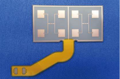
*Implementation Case: A leading communication equipment provider's 77GHz radar project demonstrated that adopting an LCP substrate + SAP process + laser-cut coverlay High Frequency FPC solution, compared to traditional MPI FPC, achieved a 22% reduction in channel insertion loss, a 40% improvement in antenna array phase consistency standard deviation, and a 15% increase in overall detection range.*