Comprehensive Analysis of PCB Technology The Ultimate Guide from Design to Manufacturing - Mastering the Invisible Engine of Next - Generation Electronic Products
Author: Jack Wang
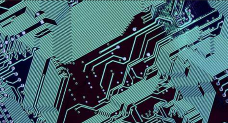
I. PCB: The "Lifeline" of Modern Electronic Devices
From smartphones to space satellites, Printed Circuit Boards (PCBs) serve as the core framework of all electronic devices. Statistics show that the global PCB market reached $89.3 billion in 2023, with an annual growth rate of 6.8% (data from Prismark). With the boom of 5G, AI, and electric vehicles, the demand for high - frequency and high - density PCBs has surged. It is predicted by Grand View Research that the PCB market for 5G base stations alone will exceed $7.4 billion by 2025.
However, an excellent PCB is far more than just "copper wires and resin." Its design accuracy, material selection, and manufacturing process directly determine the performance, lifespan, and cost of electronic products. This article will take you deep into the technical core of PCBs and reveal the most cutting - edge solutions in the industry.
II. The "Golden Rules" of PCB Design: Avoiding These 5 Fatal Mistakes
1. The "Invisible Killer" of Line Width/Line Pitch
Solutions:
①Use dynamic impedance calculation tools (such as Polar SI9000).
②Reserve a 10% line width redundancy for key signal lines.
2. The "Thermal Expansion Trap" in Via Design
Data Warning: Via - related problems account for 31% of PCB failure cases (IPC 2023 report). When the aperture ratio (hole diameter/board thickness) is < 1:8, the non - uniformity of the copper thickness on the hole wall is > 25%. Vias without teardrop pads have a dropout rate as high as 47% in thermal cycle tests.

Industry Solutions: The laser blind via + via filling and electroplating process can increase the yield rate to 92%.
III. Material Revolution: The "Performance King" of High - Frequency PCBs in 2024
1. Performance Comparison of High - Frequency Substrates
Material | Dk (10GHz) | Df (10GHz) | Thermal Conductivity (W/mK) | Cost ($/㎡) |
Rogers RO4350B | 3.48±0.05 | 0.0037 | 0.6 | 180 - 250 |
Isola I - Tera | 3.45±0.08 | 0.0031 | 0.7 | 120 - 180 |
Taiguang TG - 260 | 3.65±0.12 | 0.0045 | 0.5 | 80 - 120 |
Trend Interpretation:
①The demand for low - loss materials is surging. 5G millimeter - wave (28GHz+) requires Df < 0.005.
②Heat dissipation has become a key bottleneck. For every 1W increase in power consumption, the temperature rise of the PCB needs to be controlled within < 3℃.
2. The Rise of Environmentally Friendly Materials
①Halogen - Free Substrates: Their market share increased from 18% in 2020 to 34% in 2023.
②Biodegradable PCBs: A plant - based resin board developed by Panasonic has a natural degradation rate of 80% in 6 months.
IV. Manufacturing Processes: The Leap from "Qualified" to "Excellent"

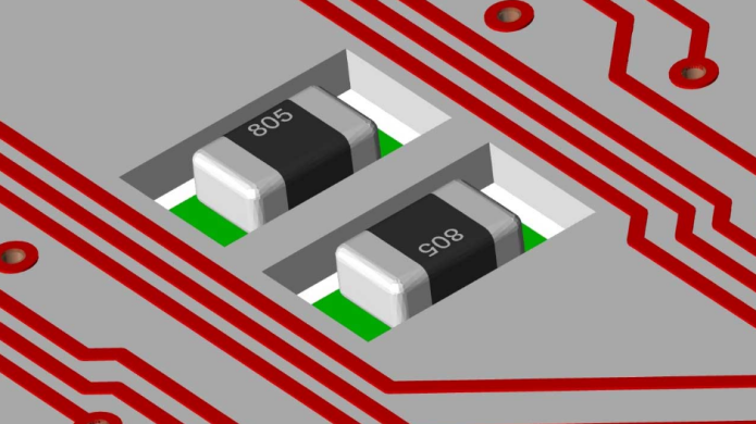
1. The Precision Revolution of SMT Soldering
Industry Benchmark: The mounting accuracy of 01005 components (0.4×0.2mm) needs to reach ±25μm.
Process | Mounting Speed (cph) | Defect Rate (ppm) |
Traditional Universal Machine | 25,000 | 150 |
Modular High - Speed Machine | 85,000 | 50 |
2. The Lifeline of the Welding Process
①Reflow Soldering Temperature Curve: The peak temperature is 245 - 255℃. When it exceeds 260℃, the void rate of BGA solder balls increases by 300%.
②Nitrogen - Protected Welding: When the oxygen content is < 500ppm, the solder joint strength is increased by 22%.
V. The Future Is Here: Three Major Breakthroughs in PCB Technology in 2025
1. PCBs with Embedded Components
Intel's latest motherboard embeds capacitors/resistors in the inner layers of the PCB, reducing signal delay by 40%. The technical difficulty lies in that the inter - layer alignment accuracy needs to be < 5μm.
2. 3D - Printed PCBs
Nano Dimension's DragonFly IV supports the printing of 10 - layer boards with a line width/line pitch of 20/20μm. In small - batch production, it can save 60% of costs compared to traditional processes.

3. Photonic Integrated Circuits (PICs)
Silicon - photonics PCBs have a data transmission rate exceeding 1Tbps and a power consumption reduction of 80%. They are applied in data center optical modules and autonomous driving LiDARs.

VI. Practical Guide: How to Choose a Reliable PCB Manufacturer?
1. Key Certification List
2. Identifying Cost Traps
The Truth Behind Low Prices: A certain customer chose a manufacturer with a 15% lower quote. Eventually, due to impedance out of control, the products were recalled, resulting in losses exceeding $500,000.
Reasonable Cost Structure (Taking a 6 - layer board as an example):
Item | Proportion |
Material Cost | 55% |
Equipment Depreciation | 20% |
Process Control | 15% |
Profit | 10% |
Data sources: IPC global reports, Prismark market analysis, and actual measurements from the PCBMASTER laboratory.
Author: Jack Wang