Copper-based PCB Design: Principles, Key Points and Innovative Practices
Abstract: This article delves into the relevant technologies of copper-based PCB (Printed Circuit Board) design. Starting from the basic concepts and characteristics of copper-based PCBs, it elaborates on their advantages in thermal management, electrical performance and other aspects in detail. It further analyzes the key points in copper-based PCB design, including laminate structure design, routing planning, via design, etc., and combines practical cases to analyze common problems and solution strategies in the design process. Meanwhile, it explores the application trends and innovative practices of copper-based PCBs in emerging technology fields such as high-power electronic equipment and LED lighting, providing a comprehensive technical reference and guidance for electronics engineers in copper-based PCB design work.
I. Introduction
With the rapid development of electronic technology, electronic equipment is constantly evolving towards miniaturization, high performance and high power density. In this process, as the platform for carrying and connecting electronic components, PCBs are facing increasingly stringent performance requirements. Copper-based PCBs, with their excellent thermal conductivity, good electrical characteristics and relatively high mechanical strength, have been widely used in numerous fields. In-depth research on copper-based PCB design technology is of great significance for improving the overall performance and reliability of electronic equipment.
II. Characteristics of Copper-based PCBs
(I) Excellent Thermal Conductivity
Copper is a metal material with extremely high thermal conductivity, with a thermal conductivity of approximately 400 W/(m·K). In copper-based PCBs, the copper layer can quickly and effectively conduct the heat generated by electronic components out, thereby reducing the operating temperature of the components and improving the stability and service life of the equipment. For example, in the application of high-power semiconductor devices, copper-based PCBs can quickly dissipate the heat generated by chips, avoiding the degradation or even damage of device performance caused by overheating.
(II) Good Electrical Performance
Copper has a relatively low resistivity, approximately 1.7×10⁻⁸Ω·m. This enables copper-based PCBs to reduce signal loss and distortion during signal transmission, ensuring the integrity and accuracy of signals. For circuits with high-frequency and high-speed signal transmission, such as communication base station equipment and high-speed computer motherboards, copper-based PCBs can provide stable and reliable electrical connections to meet their strict requirements for signal quality.
(III) Relatively High Mechanical Strength
The copper layer of copper-based PCBs endows the circuit board with relatively high mechanical strength and rigidity, enabling it to withstand relatively large mechanical stresses and vibrations. In some application scenarios where high mechanical performance of the circuit board is required, such as automotive electronics and aerospace electronic equipment, copper-based PCBs can better protect electronic components and prevent damage caused by mechanical impacts.
III. Key Points in Copper-based PCB Design
(I) Laminate Structure Design
1. Determination of the Number of Layers and Copper Layer Distribution
The number of layers of the PCB is determined according to the functional complexity of the circuit, electrical performance requirements and heat dissipation needs. For simple low-power circuits, fewer layers may be adopted, such as 2 - 4 layers; while for complex high-power and high-speed signal transmission circuits, 6 or more layers may be required. In terms of copper layer distribution, usually, the thicker copper layer is set in the area close to the heat source or where good heat dissipation is needed to enhance the heat dissipation effect. For example, in the design of a power module, the power layer (thick copper layer) is placed on the layer in close contact with power devices for efficient heat dissipation.
2. Selection of Dielectric Layer Materials and Thickness Control
The selection of dielectric layer materials will affect the electrical and thermal performance of the PCB. Common dielectric layer materials include FR - 4, polyimide, etc. FR - 4 has good comprehensive performance and a moderate price, and is suitable for general copper-based PCB design; polyimide has higher heat resistance and dielectric properties and is suitable for high-temperature or high-frequency application scenarios. The thickness of the dielectric layer needs to be precisely controlled. A thinner dielectric layer can reduce the signal transmission delay but may increase the interlayer capacitance; a thicker dielectric layer has the opposite effect. In the design of high-speed signal transmission lines, the thickness of the dielectric layer needs to be optimized according to the frequency and transmission speed of the signal to balance the influence of signal delay and interlayer capacitance.
(II) Routing Planning
1. Power Line and Ground Line Design
The design of power lines and ground lines is crucial for the electrical performance and stability of copper-based PCBs. The power lines should have sufficient width to meet the current requirements of the circuit and reduce the voltage drop on the lines. The minimum width of the power lines can be determined by calculation according to the current magnitude and copper foil thickness. For example, for a current of 1 A, if the copper foil thickness is 35 μm, the width of the power line may need to be about 0.5 mm. The ground lines should adopt the method of large-area copper plating as much as possible to form a good ground plane, reduce the ground impedance and noise interference. Meanwhile, in multi-layer PCBs, dedicated ground layers can be set, and multiple ground layers can be connected through vias to enhance the grounding effect.
2. Signal Routing Principles
For high-speed signal routing, the line length should be shortened as much as possible to reduce the signal transmission delay and reflection. The equal-length routing technique should be adopted to ensure the length matching of differential signal pairs and improve the signal quality. For example, in the design of a high-speed USB interface circuit, the length difference of differential signal pairs should be controlled within a certain range (such as within 5 mil). In addition, signal routing should avoid acute-angle intersections with power lines and ground lines to reduce electromagnetic interference. During layout and routing, the signal flow and priority should also be reasonably planned, and important signal lines should be arranged in areas with less interference.
(III) Via Design
1. Selection of Via Types
Common via types used in copper-based PCBs include through vias, blind vias and buried vias. Through vias penetrate through all layers of the PCB. Their processing technology is simple, but they will occupy more PCB space and may introduce relatively large inductance during high-frequency signal transmission. Blind vias extend from one surface of the PCB to a certain internal layer, and buried vias are located between the internal layers of the PCB. Blind vias and buried vias can reduce the size of the PCB and have better high-frequency performance than through vias. In the design of high-speed multi-layer copper-based PCBs, for key high-speed signal lines, blind vias or buried vias can be preferentially selected to achieve interlayer connections to improve signal integrity.
2. Optimization of Via Size and Parameters
The size of vias includes parameters such as hole diameter and pad diameter. The size of the hole diameter will affect the processing difficulty and cost of vias, as well as their electrical performance. A smaller hole diameter can reduce the parasitic capacitance and inductance of vias, but the processing difficulty is relatively large. The pad diameter should be determined according to the hole diameter and the manufacturing process requirements of the PCB. Generally, the pad diameter should be larger than the hole diameter by a certain proportion (such as 0.2 - 0.3 mm) to ensure the reliability of vias. In the design of high-frequency signal transmission vias, the parasitic parameters of vias need to be calculated and optimized in detail. For example, the anti-pad size of vias can be adjusted to reduce parasitic capacitance.
IV. Common Problems and Solution Strategies in Copper-based PCB Design
(I) Heat Dissipation Problems
1. Problem Manifestation
In copper-based PCB design, if the heat dissipation design is unreasonable, it may lead to the overheating of electronic components during operation, affecting their performance and reliability. For example, in a high-power density power circuit, the heat generated by power devices cannot be dissipated in time, which may cause the junction temperature of the devices to exceed the allowable range, resulting in device failure.
2. Solution Strategies
Optimize the thickness and distribution of the copper layer to increase the heat dissipation area. For example, set a large-area copper heat sink under power devices and conduct heat to other copper layers through thermal vias for further dissipation. Combine heat dissipation accessories such as heat dissipation fins and heat pipes with copper-based PCBs to improve heat dissipation efficiency. For example, in the design of some server motherboards, heat pipes are connected to copper-based PCBs to quickly conduct heat to the heat dissipation fins outside the chassis. In addition, the layout of the PCB can also be optimized to minimize the thermal resistance between the heat source and the heat dissipation channel. For example, place components with large heat generation near the edge of the PCB or in areas with good ventilation.
(II) Signal Integrity Problems
1. Problem Manifestation
When high-speed signals are transmitted on copper-based PCBs, signal integrity problems such as signal reflection, crosstalk and delay may occur. For example, when the impedance of a signal transmission line is not matched, signal reflection will occur at the end of the transmission line, resulting in signal distortion; electromagnetic coupling between adjacent signal lines will cause crosstalk and affect the normal transmission of signals.
2. Solution Strategies
Conduct precise impedance matching design by adjusting parameters such as the width of the transmission line, the thickness of the dielectric layer and the thickness of the copper foil to make the characteristic impedance of the transmission line match the impedance of the signal source and the load. For example, when designing a high-speed signal transmission line with an impedance of 50 Ω, calculate the appropriate line width and dielectric layer thickness according to the PCB materials and process parameters. Adopt shielding measures to reduce crosstalk, such as setting grounded shielding lines between sensitive signal lines or using shielding layers. For multi-layer PCBs, the ground layer can be used as a shielding layer with the signal layer sandwiched in the middle. Meanwhile, follow the signal integrity design rules during layout and routing, such as maintaining the spacing between signal lines and avoiding excessive parallel routing.
(III) Manufacturing Process Compatibility Problems
1. Problem Manifestation
Some special design requirements of copper-based PCBs may not be compatible with the PCB manufacturing process, resulting in defects or rejects during the manufacturing process. For example, if the size of vias is too small or the shape is too complex, problems may occur in manufacturing processes such as drilling and electroplating; uneven copper layer thickness may affect the etching effect of the PCB.
2. Solution Strategies
Fully communicate with the PCB manufacturer during the design stage to understand its manufacturing process capabilities and limitations. Adjust the design parameters, such as via size and copper layer thickness, according to the manufacturer's suggestions. For example, if the minimum hole diameter of the manufacturer's drilling process is 0.2 mm, vias smaller than this size should be avoided in the design. Conduct Design for Manufacturability (DFM) checks on the PCB design, and use professional DFM software or tools to identify potential manufacturing process problems in advance and make modifications. For example, check the connectivity of the copper layer and whether there are isolated copper areas to ensure the reliability of the PCB during the manufacturing process.
V. Application Trends and Innovative Practices of Copper-based PCBs in Emerging Technology Fields
(I) High-power Electronic Equipment
1. Application Scenarios and Requirements
In high-power electronic equipment such as electric vehicle charging piles and solar inverters, copper-based PCBs can meet the heat dissipation and electrical connection requirements of high current and high power density. For example, electric vehicle charging piles need to provide a large amount of electrical energy to electric vehicle batteries in a short time, and the internal power modules will generate a large amount of heat. Copper-based PCBs can effectively dissipate the heat while ensuring the stable transmission of large currents.
2. Innovative Practices
Adopt a multi-layer copper-based PCB structure and combine it with new heat dissipation materials and technologies, such as nano-carbon material heat dissipation coatings and phase change material heat dissipation technologies, to further improve heat dissipation efficiency. For example, in the design of copper-based PCBs for solar inverters, nano-carbon material heat dissipation coatings are applied to the surface of the copper layer to enhance its heat dissipation ability. Develop high-power density copper-based PCB design schemes, optimize circuit layout and component selection to reduce the volume and weight of PCBs and increase power density. For example, adopt an integrated power module design, integrating multiple power devices and passive components on a copper-based PCB, reducing the length and resistance of connection lines and improving the efficiency and reliability of the system.
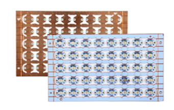
(II) LED Lighting
1. Application Scenarios and Requirements
In the field of LED lighting, copper-based PCBs are mainly used in the design of LED light boards. LEDs will generate a certain amount of heat during operation. If the heat dissipation is poor, it will lead to increased light attenuation and shortened lifespan of LEDs. Copper-based PCBs can provide a good heat dissipation platform for LEDs to ensure their normal operation and long lifespan. For example, copper-based PCBs are widely used in indoor lighting LED light boards and outdoor large LED display screens.
2. Innovative Practices
Design special copper-based PCB structures, such as setting heat dissipation copper columns or copper grooves under LED beads to increase the heat dissipation area and heat conduction path. For example, some high-end LED lighting products adopt a design combining copper-based PCBs and heat dissipation copper columns to quickly conduct the heat generated by LEDs to the surrounding environment. Adopt flexible copper-based PCB technology to meet the flexible design requirements of LED lighting products, such as bendable LED light strips. Flexible copper-based PCBs can realize the diversified design of LED lighting products while ensuring heat dissipation and electrical performance, expanding their application range.
VI. Conclusion
Copper-based PCB design technology occupies an important position in the field of modern electronic technology. By deeply understanding the characteristics of copper-based PCBs, mastering the key points of their design, effectively solving common problems in design, and paying attention to the application trends and innovative practices in emerging technology fields, electronics engineers can design copper-based PCBs with excellent performance, reliability and stability, providing strong technical support for the development of various electronic equipment. With the continuous progress of electronic technology, copper-based PCB design technology will also continue to innovate and develop and play a more important role in the field of electronic engineering in the future.