


Multilayer PCBs A Core Technology in the Evolving Electronics Landscape
As electronic devices continue to trend towards miniaturization while demanding higher functionality, speed, and reliability, multilayer printed circuit boards (PCBs) have emerged to meet these challenges. This article provides a comprehensive exploration of multilayer PCBs, covering their fundamental advantages, disadvantages, cost structure, critical design considerations, and complex manufacturing processes.
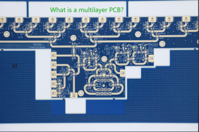
As the name implies, a multilayer PCB consists of three or more conductive layers. These layers are composed of copper foil separated by insulating dielectric layers. The entire structure is laminated together under high pressure and temperature to form a single, monolithic unit. Within these layers, some serve as signal layers for transmitting electrical signals, others as power planes for distributing power, and others as ground planes, acting as common electrical reference points.
Typically, multilayer PCBs range from 4 layers up to 60 layers or more, depending on application complexity. However, the most common configurations are between 4 and 16 layers. Each layer plays a crucial role in enabling the PCB to fulfill its intended function, whether in simple consumer electronics or highly complex aerospace systems.
nterlayer connection technology is a key differentiator in multilayer board sophistication:
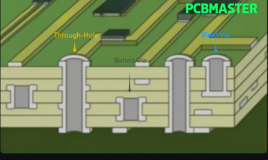
·Through-Hole Vias: Connect all layers from top to bottom.
·Blind Vias: Connect an outer layer to an inner layer without penetrating the entire board.
·Buried Vias: Connect only internal layers, hidden within the board structure.
1. Increased Component and Trace Density:
A primary advantage is the ability to accommodate significantly higher component and trace density compared to single or double-sided PCBs. While single-sided boards are limited to one surface and double-sided to two surfaces, multilayer PCBs enable vertical routing across multiple layers. This allows complex circuits to be compressed into smaller physical spaces. For instance, smartphones, highly compact devices packed with numerous components and intricate circuits, rely indispensably on multilayer PCBs. Processors, memory chips, wireless modules, and various other components interconnect across the board's layers, enabling all functionality within a slim form factor.
2. Enhanced Electrical Performance:
Multilayer PCBs offer superior electrical characteristics in several ways:
·Signal Integrity: Careful stackup design allows critical traces to be embedded between ground planes. These planes act as shields, protecting signal traces from electromagnetic interference (EMI) and radio frequency interference (RFI) noise. This shielding preserves signal integrity, ensuring accurate transmission, especially crucial in high-speed and high-frequency applications. For example, in high-speed data transfer applications like USB 3.0 or Ethernet, multilayer PCBs with proper signal isolation prevent signal degradation.
·Impedance Control: Multilayer PCBs facilitate precise impedance control. The impedance of transmission lines (like PCB traces) is vital for ensuring signal transmission without reflection. By controlling dielectric thickness, trace width, and spacing between adjacent traces, designers can fine-tune impedance to match component and circuit requirements. This is particularly critical in high-performance computing where high-speed data buses must operate with minimal signal distortion.
3. Enabling Device Miniaturization:
The ability to integrate more components and connections vertically has been instrumental in driving electronic device miniaturization. In today's market demanding smaller, more portable devices, multilayer PCBs make this possible. Wearable devices, such as smartwatches and fitness trackers, exemplify this. These devices need to house various components—sensors, processors, wireless communication modules—within a tiny space. Multilayer PCBs enable the compact and efficient integration of all these elements, making wearable technology a reality.
4. Increased Functionality on a Single Board:
Multilayer PCBs allow the consolidation of multiple functions onto a single board. Instead of using several single or double-sided PCBs interconnected, one multilayer PCB can perform all necessary functions. This reduces the overall size and weight of the end product and simplifies the assembly process. For example, modern automotive infotainment systems require audio processing, video display, and wireless connectivity; a multilayer PCB integrates all these functions, enabling a leaner, more reliable design.
5. Reduced Need for Connectors:
By transmitting signals and power across multiple layers internally, the need for external connectors between different boards is significantly reduced or even eliminated. Traditional designs using multiple single or double-sided PCBs required numerous connectors for electrical interconnection. These connectors can be sources of reliability issues, such as loosening or corrosion. Multilayer PCBs minimize connector usage by integrating functionality onto a single board, simplifying the structure and reducing product weight. This is especially advantageous in applications like aerospace and satellite electronics with strict space and weight constraints.
6. Structural Variety (Rigid and Flexible Options):
Multilayer PCBs are available in both rigid and flexible constructions. Rigid multilayer PCBs are the most common, suitable for a wide range of applications requiring a solid, stable platform for component mounting. Flexible multilayer PCBs, on the other hand, offer unique advantages in applications where the PCB must bend or conform to a specific shape. For instance, flexible multilayer PCBs can be used in laptop hinge areas to connect the display to the main body, allowing smooth opening and closing while maintaining reliable electrical connections. Note, however, that increasing layer count in flexible PCBs can slightly reduce flexibility.
Performance Comparison of PCBs by Layer Count
Feature | Single Layer | Double Layer | 4-Layer | 8-Layer | 12-Layer+ |
Routing Density | 1× | 1.8× | 3.5× | 6× | 10×+ |
Signal Integrity | Poor | Moderate | Good | Excellent | Outstanding |
Thermal Management | Low | Medium | Medium-High | High | Very High |
Typical Applications | LED Lighting | Power Modules | Industrial | Mobile Phone | Servers/ |
|
|
| Control | Motherboard | Base Stations |
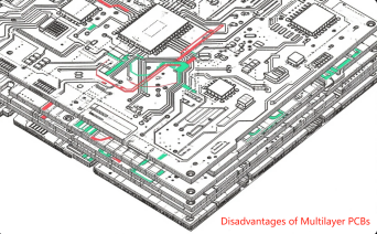
Disadvantages of Multilayer PCBs
1.Higher Cost:
·Complex Manufacturing: The most significant drawback is cost. Manufacturing multilayer PCBs is far more complex than single or double-sided boards. It involves multiple steps like creating and etching multiple inner layers, precisely laminating these layers together, and creating vias (electrical connections between layers). Each step requires specialized equipment and skilled labor, increasing costs. For example, the lamination process requires tightly controlled temperature and pressure conditions to ensure good bonding. Any deviation can lead to board defects, increasing overall costs due to rework or scrap.
·Material Cost: Multilayer PCBs often require higher-quality materials. High-performance applications may demand materials like high-Tg FR-4 or polyimide, which offer better thermal stability and electrical properties but are more expensive than standard PCB materials. Additionally, increased layer count requires more material, further raising costs.
·Economies of Scale: While higher production volumes can reduce per-unit costs, the initial investment in tooling and setup for multilayer PCB production is relatively high. The cost of small-batch production can be particularly high as fixed setup and tooling costs are amortized over fewer units.
2.Limited Supplier Availability:
Not all PCB manufacturers have the capability or resources to produce multilayer PCBs. The requirements for specialized equipment, skilled labor, and stringent quality control make it difficult for many smaller manufacturers to enter this space. Consequently, PCB designers may have fewer choices when selecting a manufacturer for their multilayer PCB projects. Lack of competition in certain regions can also lead to higher costs.
3.Design Complexity:
·Crosstalk and Impedance Issues: High compactness introduces design challenges. Crosstalk (interference between adjacent signal traces) can be a significant problem. As traces run closer together across multiple layers, careful design is needed to minimize crosstalk. Furthermore, impedance control, while an advantage for electrical performance, adds design complexity. Designers must consider trace width, spacing, and dielectric thickness to ensure proper impedance matching. Any miscalculation can lead to signal integrity issues.
·Thermal Management: Multilayer PCBs in high-power applications generate substantial heat. Insulating dielectric layers create higher thermal resistance, making heat dissipation more difficult. This necessitates careful thermal design, including the use of thermal vias, dedicated ground planes for heat spreading, and strategic component placement. Designers must perform thermal simulations to ensure the PCB operates within acceptable temperature ranges.
4.Longer Lead Times and Higher Testing Requirements:
·Manufacturing Lead Time: The complex manufacturing process typically results in longer lead times compared to simpler boards. Each step—from inner layer fabrication to lamination and drilling—requires time and precision. Delays or issues at any step can further extend production time. For instance, layer misalignment during lamination may require rework, adding days to the schedule.
·Testing Requirements: Increased functionality and complexity demand more extensive testing. Electrical testing is essential to verify all connections between layers are correct and free of shorts or opens. Automated Optical Inspection (AOI) is commonly used to check for physical defects like layer misalignment or incomplete etching. For high-reliability applications, more advanced techniques like X-ray inspection may be necessary to ensure internal layer integrity. This extensive testing adds to the overall cost and production time.
5.Difficulty in Repair and Rework: Once components are soldered onto a multilayer PCB, repair and rework can be extremely difficult, sometimes impossible. The layered structure and complex internal connections make accessing and fixing problems challenging. For example, a short circuit buried between internal layers may be nearly impossible to isolate and repair without damaging other parts of the board. In such cases, replacing the entire board may be necessary, which can be costly in high-value applications.
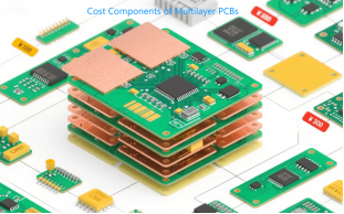
The cost of a multilayer PCB is influenced by several key factors:
1.Layer Count and Complexity:
·Material and Labor Costs: As PCB layer count increases, so does the amount of material required. Each additional layer means more copper foil, dielectric material, and prepreg. This directly increases material costs. Moreover, manufacturing becomes more complex. Creating and etching additional layers, aligning them during lamination, and drilling through multiple layers involve more steps. These extra steps require more time and skilled labor, increasing labor costs. For example, a 4-layer PCB will typically cost less than a 10-layer PCB due to differences in material usage and manufacturing complexity.
·Complex Circuit Design: Highly complex circuit designs on multilayer PCBs, featuring fine-pitch traces, high-density interconnects (HDI), or intricate routing requirements, also increase costs. Such designs often require more precise manufacturing processes and advanced equipment, which are more expensive to operate and maintain.
2.Materials Used:
·Substrate Material: The choice of substrate material significantly impacts cost. Standard materials like FR-4 are relatively inexpensive and common. However, high-performance applications may require materials like Rogers laminates (excellent electrical properties for high-frequency use) or polyimide (known for high-temperature resistance). These specialty materials can cost several times more than FR-4. Brand and quality of the substrate material also affect cost.
·Copper Foil Weight: The thickness (weight) of the copper foil used in the PCB affects cost. Thicker copper foils are often used for applications requiring higher current-carrying capacity, like power circuits. As thicker copper is more expensive, its use increases the overall PCB cost.
3.Production Volume:
Economies of scale play a crucial role. In high-volume production, fixed costs associated with setup, tooling, and equipment depreciation are spread over more units, reducing the per-unit cost. For instance, the unit cost for manufacturing 1000 units of a specific multilayer PCB will be higher than for 10,000 units. For large volumes, manufacturers can also negotiate better prices with material suppliers, further reducing costs.
Technical Specifications:
Advanced Manufacturing Techniques: Using techniques like High-Density Interconnect (HDI) technology or incorporating microvias significantly increases multilayer PCB cost. HDI allows higher component density and complex routing but requires specialized equipment and more precise processes. Microvias, very small vias connecting layers, are harder to manufacture than standard vias, adding to the cost.
4. Impedance Control and Other Special Features:If the PCB requires strict impedance control (common in high-speed/high-frequency applications), additional manufacturing steps are needed to ensure requirements are met. This may include tighter control over trace width, dielectric thickness, and the use of special materials, all adding cost. Other special features like blind and buried vias (connecting non-adjacent layers) also increase manufacturing complexity and cost.
Multilayer PCB Cost Structure Comparison (Example: 10cm x 10cm Board)
Cost Item | 2-Layer | 4-Layer | 8-Layer | 12-Layer |
Material Cost | $2.5 | $8.0 | $18 | $35 |
Imaging/Patterning | $1.0 | $3.5 | $7.0 | $12 |
Lamination | - | $2.5 | $6.0 | $15 |
Drilling | $0.8 | $1.5 | $3.5 | $8.0 |
Surface Finish | $1.2 | $1.2 | $1.5 | $1.8 |
Testing | $0.5 | $1.8 | $4.5 | $12 |
Total | $6.0 | $18.5 | $40.5 | $83.8 |
Multilayer PCB Design Considerations
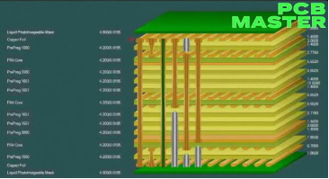
Typical 8-Layer Stackup Structure:
Layer Order | Function | Thickness (mm) | Remarks |
L1 | Signal | 0.035 | High-Speed Signals |
L2 | Ground Plane | 0.2 | Solid Plane |
L3 | Signal | 0.035 | Stripline Routing |
L4 | Power Plane | 0.2 | Core Power |
L5 | Power Plane | 0.2 | I/O Power |
L6 | Signal | 0.035 | Stripline Routing |
L7 | Ground Plane | 0.2 | Solid Plane |
L8 | Signal/Pads | 0.035 | Connectors/Components |
1.Layer Configuration:
·Determining Layer Count: The first step is determining the appropriate number of layers based on circuit complexity and application electrical requirements. Simple circuits with few components might only need a 4-layer PCB, while complex applications like high-performance computing or telecommunications may require 6, 8, or more layers due to numerous high-speed signals and power distribution needs.
·Layer Stackup Order: The sequence of layers is critical. Signal layers should be positioned to minimize interference. Embedding critical traces between ground planes is common practice; these planes act as shields against EMI/RFI. In a typical 4-layer PCB, the top and bottom layers may be used for components and some routing, while the internal layers serve as power and ground planes. The exact arrangement depends on signal nature and power distribution requirements.
2.Material Selection:
·Electrical Performance: Material choice depends on electrical requirements. High-frequency applications favor materials with low dielectric constant (Dk) and low dissipation factor (Df), such as Rogers RO4000 series or certain polyimides, ensuring signal integrity and minimizing loss. For high-temperature environments, materials with a high glass transition temperature (Tg) are essential (e.g., high-Tg FR-4, ceramic-filled materials) to withstand heat without deformation.
·Mechanical Properties: Mechanical properties must also be considered. Substrates must withstand manufacturing and operational stresses. Applications involving vibration or shock require materials with good mechanical strength and, if applicable, flexibility.
3.Trace and Spacing Management:
·Trace Width: Width is determined by the current it must carry. Power circuits handling several amps require wider traces to prevent overheating and voltage drop than signal traces carrying milliamps. Trace width also affects transmission line impedance, requiring careful design.
·Trace Spacing: Adequate spacing between traces is crucial to prevent crosstalk. In high-speed circuits, spacing must be carefully calculated based on signal frequency and amplitude; closer traces increase crosstalk risk. Design rules and simulation tools are used to determine appropriate spacing.
4.Via Selection:
·Through-Hole Vias: Simplest type, penetrating the entire board. Relatively easy to manufacture, used where cost is primary. However, they consume more space.
·Blind Vias: Connect an outer layer to an adjacent inner layer. Help reduce overall PCB size. Manufacturing is more complex and costly than through-hole vias. Common in space-constrained devices like mobiles.
·Buried Vias: Connect non-adjacent internal layers. Used to optimize routing and component layout. Hidden within the board, they require precise manufacturing for accurate connection, adding cost due to extra steps. Designers must balance compactness needs against manufacturability and cost.
5.Symmetry and Balance:
·Stackup Symmetry: The layer stackup should be symmetrical around the central core. This symmetry balances mechanical and electrical properties. Asymmetry in insulation and copper thickness on either side of the center can cause warpage during manufacturing or use. Symmetry also aids impedance control.
·Component Placement: Placement should consider weight distribution and thermal dissipation. Distributing heavy components evenly prevents board bending. Spacing high-power components and placing them near cooling areas helps manage heat accumulation, especially critical in large multilayer PCBs or those with high-power components.
6.Thermal Management Design:
Compact structures and high component density create thermal challenges. Strategies include:
·Thermal Vias: Placed under heat-generating components, connecting copper areas to internal ground/power planes, spreading heat.
·Large Copper Areas: Ground and power planes with large copper pours act as heat spreaders.
·Component Layout: Spacing high-power components apart and near board edges/cooling zones prevents hotspots.
·Thermal Interface Materials: Thermal pads or pastes may be needed to conduct heat from the PCB to external heatsinks.
7.Design Verification and Simulation:
Essential steps in the design process include:
·Signal Integrity (SI) Simulation: Ensures high-speed signals transmit without excessive attenuation or reflection.
·Thermal Simulation: Predicts hotspots and validates thermal management strategies.
·Electromagnetic Compatibility (EMC) Simulation: Ensures the PCB meets EMI/RFI standards and doesn't interfere with, or suffer from, other devices.
·Design Rule Check (DRC): Verifies compliance with manufacturing constraints and design rules before release, reducing errors and rework.
Multilayer PCB Manufacturing Process
Multilayer PCB production is a complex, multi-step process demanding high precision and strict quality control. Key steps are detailed below:
1.Inner Layer Fabrication:
·Substrate Cutting: Large substrate sheets (e.g., FR-4) are cut to required panel sizes.
·Photoresist Application: Photoresist is applied to the copper surface (spraying, dipping, dry film lamination).
·Exposure: Panels are exposed to UV light through photomasks containing the inner layer circuit pattern.
·Development: Exposed panels are developed, removing unexposed (negative resist) or exposed (positive resist) photoresist, leaving the circuit pattern.
·Etching: Panels are etched (e.g., ferric chloride, ammonium persulfate) to remove unprotected copper, forming the copper circuit.
·Stripping: Remaining photoresist is stripped, revealing the copper circuit.
·Inner Layer AOI: Automated Optical Inspection checks for defects (shorts, opens, under-etching). Defective panels are reworked or scrapped.
2.Oxide Treatment (Browning/Blackening):
After fabrication, inner layers undergo oxide treatment to form a thin oxide layer on the copper surface, enhancing adhesion to prepreg during lamination. Treated panels are thoroughly cleaned.
3.Stackup Preparation:
·Stackup Configuration: Layer sequence (inner layers, prepreg, outer copper foil) is determined per design.
·Alignment Marks: Marks are added to inner layers for precise alignment during lamination.
·Prepreg Placement: Prepreg sheets (pre-impregnated with resin) are placed between inner layers and under outer foil. Quantity and type depend on required thickness and properties.
4.Lamination:
The stack is placed in a lamination press under high temperature (typically 170-180°C) and pressure (200-400 psi). Prepreg resin melts, flows, and bonds the layers. Precise control is critical for:
·Complete bonding between all layers.
·Absence of trapped air bubbles (voids).
·Precise layer alignment ensuring via/trace connectivity.
Panels are cooled after lamination.
5.Drilling:
Precision drilling machines create vias (through-hole, blind, buried) using X-ray systems for inner layer alignment if needed (especially blind/buried). Holes are deburred and cleaned.
6.Hole Metallization (Plated Through Hole - PTH Process):
To make vias conductive:
·Deburring & Cleaning: Remove drilling debris, clean for adhesion.
·Electroless Copper Deposition: A thin conductive copper layer is chemically deposited onto hole walls.
·Electrolytic Copper Plating: Copper thickness on hole walls and outer surfaces is increased for conductivity and mechanical strength.
7.Outer Layer Fabrication:
Similar to inner layers:
·Photoresist Application: Applied to outer copper.
·Exposure & Development: Using outer layer pattern photomasks.
·Etching: Removal of unprotected copper.
·Stripping: Removal of remaining photoresist.
8.Solder Mask Application:
An insulating layer (typically green, other colors available) is applied, leaving only pads and areas to be soldered exposed. Protects copper, prevents shorts, provides mechanical protection. Applied via screen printing or photoimaging.
9.Silkscreen (Legend Printing):
Text, symbols, and markings (component designators, polarity, logos) are printed on the PCB surface (usually white or black ink) to aid assembly and servicing.
10.Surface Finish:
Applied to exposed copper pads to protect against oxidation and ensure solderability. Common types:
·HASL (Hot Air Solder Leveling): Tin-lead or lead-free solder coating.
·ENIG (Electroless Nickel Immersion Gold): Nickel barrier layer with gold finish. Excellent solderability/corrosion resistance.
·Immersion Silver / Immersion Tin: Lead-free alternatives.
·OSP (Organic Solderability Preservative): Thin organic coating protecting copper until soldering.
11.Final Testing and Inspection:
Electrical Testing: Continuity (shorts/opens) testing using flying probe or bed-of-nails testers.
·AOI: Re-checking outer layers, solder mask, silkscreen.
·X-ray Inspection: For complex boards, checks internal connections/via integrity (especially blind/buried).
·Impedance Testing: Verifies impedance meets specifications where controlled.
12.Panel Depanelization (Singulation): Individual PCBs are separated from the manufacturing panel using methods like routing, punching, or laser cutting
Industry Applications & Selection Guide
Consumer Electronics:
·Smartphones: 10-12 layer HDI boards, trace/space ≤3/3mil.
·TWS Earbuds: 6-layer rigid-flex PCBs, bend radius <2mm.
·Game Consoles: 8-layer boards with 2oz power planes, supporting 200W+ transient power.
Industrial Control:
·PLC Modules: 6-layer boards with 4kV isolation slots, operating temp -40~105°C.
·Motor Drives: Heavy-copper boards (4oz+) carrying 50A peak current.
Automotive Electronics:
ECU Controllers: 6-8 layer boards, compliant with AEC-Q100.
LiDAR: High-frequency laminates (Df <0.003), for 24GHz radar applications.
Medical Devices:
·Endoscopes: 12-layer HDI flexible PCBs, thickness ≤0.3mm.
·Pacemakers: Biocompatible encapsulation, operational lifespan >10 years.
Conclusion
Multilayer PCBs are pivotal in enabling the miniaturization, high performance, and multifunctionality of modern electronic devices. While they are more costly and complex to design and manufacture than single or double-sided PCBs, the advantages they offer are irreplaceable in many applications. By understanding the advantages, disadvantages, cost factors, design considerations, and production processes of multilayer PCBs, designers and manufacturers can make informed decisions to develop efficient, reliable electronic products tailored to specific needs. As technology advances, multilayer PCBs will continue to evolve, offering higher performance and smaller sizes, driving further innovation in the electronics industry.
FAQs
Q: Why are high-Tg materials predominantly used for high-layer-count PCBs?
A: The glass transition temperature (Tg) is a critical parameter for PCB substrate materials, indicating the temperature threshold at which the material transitions from a rigid solid to an elastic state. High-layer-count PCBs require high-Tg materials (typically Tg ≥170°C) for two main reasons:
·High Power Density & Heat: More layers and higher power density lead to significant heat generation during operation. High-Tg materials maintain structural stability at elevated temperatures, preventing warping or delamination.
·Manufacturing Thermal Stress: The manufacturing process involves multiple high-temperature lamination cycles. High-Tg materials offer superior resistance to thermal shock, reducing production defects like voids or cracking.
Q: What are the key principles in the stackup design of high-layer-count PCBs?
A: Stackup design critically impacts signal integrity, thermal management, and mechanical stability. Core principles include:
·Symmetry: The stackup must be symmetrical around the central core (e.g., Signal - Dielectric - Ground - Dielectric - Signal). This prevents warping caused by uneven thermal stress.
·Ground/Power Plane Optimization: High-speed signal layers should be adjacent to ground planes (forming microstrip or stripline structures) to minimize EMI. Power planes should be paired with adjacent ground planes to reduce power supply noise.
·Impedance Control: Based on signal speed (e.g., >10Gbps), target impedance values (e.g., 50Ω, 100Ω) are preset. This is achieved by precisely controlling dielectric thickness, trace width, and copper thickness.
·Thermal Layer Planning: High-power areas should incorporate large copper planes (e.g., ground planes doubling as heat spreaders) supplemented by thermal vias for heat dissipation.
Q: What are the special requirements for via design in high-layer-count PCBs?
A: Vias are critical for layer interconnection in high-layer-count PCBs. Design requirements include:
·Type Selection: Blind vias and buried vias are prioritized over through-hole vias to conserve routing space. Microvias (diameter ≤0.15mm) are often used in high-frequency designs to minimize signal reflections.
·Anti-Interference Design: Vias require "ground pads" (isolation rings) surrounding them to prevent coupling with adjacent signal layers. Dense via areas need dispersed placement to avoid impedance discontinuities.
·Reliability: Via copper plating thickness must be ≥20μm to ensure current-carrying capacity. Layer-to-layer alignment tolerance must be ≤25μm to prevent misregistration causing open circuits.
Q: Where are the main manufacturing challenges for high-layer-count PCBs?
A: Manufacturing high-layer-count PCBs demands extreme precision and advanced equipment. Key challenges are:
·Layer-to-Layer Alignment: Increased layer count heightens the risk of cumulative misalignment during lamination. Laser or X-ray alignment systems are essential to maintain tolerances ≤±10μm.
·Dielectric Layer Control: High-frequency, high-layer-count PCBs often use ultra-thin dielectrics (e.g., 25-50μm). Preventing voids, resin starvation during lamination, and ensuring stable dielectric constant (Dk) is difficult.
·Via Metallization: High aspect ratios (depth/diameter ≥10:1) are common. Achieving uniform copper plating on deep via walls is challenging; advanced processes like pulse plating are often required.
·Testing Complexity: Internal signals cannot be directly probed. Comprehensive testing requires flying probe testing, X-ray inspection (for buried/blind vias), and impedance testing (ensuring ±10% tolerance) to guarantee quality.
Q: What are the primary factors influencing the cost of high-layer-count PCBs?
A: High-layer-count PCBs are significantly more expensive than standard multilayer boards. Key cost drivers include:
·Layer Count: Cost typically increases 30%-50% for every additional 4-6 layers due to doubling of materials and processing steps.
·Materials: High-Tg FR-4, low-loss dielectrics like Rogers laminates cost 2-5x more than standard FR-4.
·Precision Requirements: Trace/space ≤3mil (0.075mm), microvias, impedance control significantly increase fabrication costs.
·Volume: Small batches (e.g., 10-50 boards) incur very high costs (amortizing setup/NRE). Large volumes (1000+ boards) benefit from economies of scale.
Q: Why is the lead time for high-layer-count PCBs longer than for standard PCBs?
A: The complex manufacturing flow results in typical lead times of 4-8 weeks (vs. 2-4 weeks for standard multilayer boards). Reasons include:
·More processing steps (e.g., a 12-layer board requires at least 3 lamination cycles).
·More extensive quality assurance (X-ray, impedance testing, thermal stress testing).
·Longer material procurement times (high-Tg, low-loss laminates are often custom orders).
Why PCBMASTER: https://www.pcbmaster.com/why
Join US:https://www.pcbmaster.com/login

