Modern PCB Via Processing Technologies A Comprehensive Guide
Author: Jack Wang
In modern PCB design and manufacturing, vias, as key channels connecting different circuit layers, their processing technology directly affects the reliability, signal integrity, and manufacturing cost of circuit boards. With the increasing popularity of High-Density Interconnect (HDI) designs, via processing technology has evolved from a simple electrical connection function to a complex system involving precision materials science and advanced processes. This article will delve into six core via processing technologies—Tenting vias, Plugged vias with soldmask, Vias not covered, as well as resin-filled vias, copper-filled vias, and silver-filled vias—providing engineers with a comprehensive technical selection guide.
Tenting Vias: Basics, Types and Functions
·Through Via: Penetrates the entire PCB layer, used for interconnection between any layers, with the lowest manufacturing cost, widely applied in ordinary circuit boards—most PCBs primarily use Tenting vias, and even most vias in HDI PCBs are Tenting vias. Mechanical drills are typically used to create these through holes, and both the hole depth and hole size are critical parameters in via manufacturing.
·Blind Via: Connects only the surface layer to a specific inner layer without penetrating the entire board, commonly seen in HDI designs to save routing space—it is considered a Blind Via only if it is connected to the TOP or BOT layer of the PCB.
·Buried Via: Entirely hidden inside the PCB, connecting two or more intermediate layers, invisible from the top and bottom layers, used in highly complex multi-layer boards but significantly increasing process costs—completely buried inside the PCB core, invisible to the naked eye.
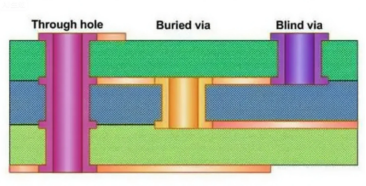
Generally, most PCBs primarily use Tenting vias, and HDI PCBs with Blind Vias and Buried Vias also mainly adopt Tenting vias. The number of Blind Vias and Buried Vias and whether they coexist depend on the design.
The structure of a via consists of a drilled hole that is subsequently plated with copper to form a plated hole, enabling electrical connections between layers. Maintaining a sufficient annular ring around the via is essential to prevent breakout and ensure reliable electrical connections.
In via-in-pad and HDI designs, the active pad in via-in-pad technology allows for direct signal transmission and improved routing density.
These vias face three core challenges in manufacturing: preventing solder migration, reducing parasitic effects, and enhancing mechanical reliability. Different processing technologies have been developed as solutions to these pain points.
When considering material compatibility and reliability, it is important to match the coefficient of thermal expansion (CTE) of the via fill to the surrounding laminate to prevent stress fractures and ensure long-term durability.
Introduction to Vias
A via is a fundamental feature in the construction of a printed circuit board (PCB), serving as a metallic drilled hole that enables the transfer of electrical signals between different layers of the circuit board. After the drilled hole is created, it is lined with a conductive material—typically a copper cylinder—to establish a reliable electrical connection. The inner layer of the via may be filled with a non-conductive material to provide additional support and prevent unwanted movement of solder or flux. Vias are especially critical in multilayer PCBs, where they allow for compact, high-density designs by connecting circuitry across various layers. This interlayer connectivity is essential for the miniaturization of electronic devices, making modern circuit boards more efficient and portable.
Via Types and Functions
In PCB design, understanding the different types of vias and their specific functions is crucial for optimizing performance and manufacturability. The three primary types are through-hole vias, blind vias, and buried vias. Through-hole vias extend from the top to the bottom of the PCB, providing a direct electrical connection between all layers and are commonly used for mounting components or connecting traces on opposite sides. Blind vias connect an outer layer to one or more internal layers without passing through the entire board, making them ideal for saving space in high-density layouts. Buried vias, meanwhile, are located entirely within the internal layers of the PCB, connecting only those layers and remaining invisible from the surface. Each via type plays a unique role in managing signal routing, layer interconnections, and overall board complexity, allowing PCB designers to tailor solutions for specific
Via Filling Materials and Conductive Options
The choice of via filling material is a key consideration in PCB fabrication, as it directly impacts the board’s thermal and electrical performance. Via filling can be achieved using either conductive or non-conductive materials. Conductive options, such as copper conductive epoxy or copper or silver epoxy, are selected when higher thermal conductivity and electrical conductivity are required—ideal for applications where efficient heat dissipation and robust signal transmission are critical. Non-conductive materials, like epoxy resin, are used primarily to provide structural support and prevent solder from wicking through the via during assembly. The selection of filling material depends on the specific needs of the circuit board: copper conductive epoxy is often preferred for its superior thermal conductivity, while silver epoxy offers a balance between conductivity and process simplicity. Non-conductive epoxy is chosen when electrical isolation is needed or when cost is a primary concern. Ultimately, the right filling material ensures the via meets both mechanical and electrical demands of the application.
Benefits of Filled Vias
Filled vias offer a range of advantages that enhance the performance and reliability of printed circuit boards. By filling vias, designers can significantly improve the thermal conductivity of the board, allowing heat to dissipate more efficiently from high-power components. Filled vias also provide enhanced electrical conductivity, ensuring stable signal transmission across layers. Structurally, filled vias reinforce the board, reducing the risk of mechanical failure and supporting the integrity of the hole walls. Another key benefit is the prevention of solder bridging during assembly, which helps avoid electrical shorts and improves yield. Additionally, filled vias minimize the risk of trapped air or moisture inside the via, which can otherwise lead to reliability issues over time. These benefits are especially important in high-density interconnect (HDI) boards, where component and trace density demand optimal heat management and signal integrity.
Via-in-Pad Design
Via-in-pad design is an advanced PCB manufacturing technique that places the via directly beneath the component pad, streamlining the path for both heat and electrical signals. This approach is particularly effective in applications requiring high thermal conductivity and electrical conductivity, such as high-power amplifiers or high-speed digital circuits. In via-in-pad designs, filled vias are essential—they are completely filled and planarized to create a uniform surface, ensuring reliable soldering and preventing solder wicking into the via during assembly. The result is a smooth, flat pad that supports robust component attachment and efficient heat transfer. Via-in-pad technology enables higher routing density and improved performance in compact, high-frequency, or high-power circuit boards.
Environmental Factors
Environmental conditions, such as temperature fluctuations and humidity, can have a significant impact on the performance and longevity of printed circuit boards. Filled vias play a vital role in protecting PCBs from these environmental stresses. By using appropriate via filling materials and techniques, designers can create a barrier that prevents moisture and contaminants from penetrating the via, thereby reducing the risk of corrosion and electrical shorts. Filled vias also help maintain the mechanical and electrical integrity of the board under thermal cycling and vibration. For PCB designers working on applications exposed to harsh environments—such as automotive, aerospace, or industrial systems—careful selection of via filling materials and the implementation of via-in-pad structures are essential strategies to ensure long-term reliability and optimal performance.
II. Detailed Explanation of Six Via Processing Technologies
1.Tenting Vias
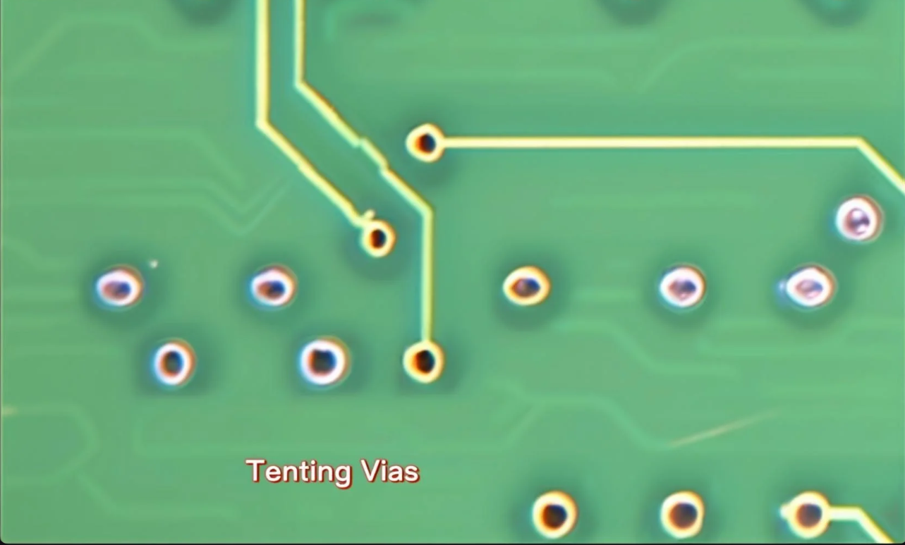
Protection is achieved by directly covering the via surface with Soldermask ink, which is the most economical processing method. Solder mask covers are applied to protect the via and enhance reliability by preventing contamination and improving long-term electrical performance.
Advantages: The soldermask layer effectively isolates moisture and contaminants to prevent copper oxidation; avoids solder paste flowing into the hole during soldering, which may cause cold solder joints; the process is simple, with almost no additional cost. Moreover, it has the highest production efficiency, and most Quick turn PCB manufacturers will recommend this method to customers for rapid delivery.
Disadvantages: The soldermask layer may expand and generate bubbles during high-temperature soldering, reducing protection; residual air in the via may cause microcracks under thermal stress. Additionally, due to insufficient filling of soldermask ink inside the hole, the ink at the via position may be less safe and reliable than that of Plugged Vias with Soldermask during long-term use.
Design Points: This technology must be adopted in BGA areas to prevent short circuits between solder balls and vias; the soldermask opening of vias in the Gerber file needs to be closed (i.e., cancel the definition of the Solder Mask layer).
2. Plugged Vias with Soldermask
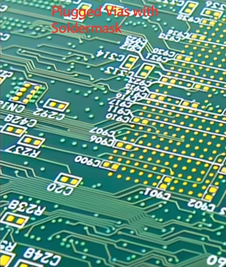
High-viscosity ink is used to fill the via interior before soldermask covering, forming a dual protection structure. LPI solder mask and solder resist, both liquid photo imageable materials, are commonly used for via fill and hole plugging to enhance via reliability and meet IPC standards.
Process Characteristics: Aluminum sheet via plugging (lower cost) or vacuum via plugging equipment (higher cost but better saturation and uniformity) is usually used to fill the vias with soldermask ink.
Advantages: Via processing on the back of wave-soldered boards to prevent solder penetration; applicable to areas with surface flatness requirements (e.g., under QFN packages). Due to the full filling of ink in the vias, the saturation of ink in the holes can be ensured, thus guaranteeing long-term functional performance and quality.
Disadvantages: Curing shrinkage may cause surface micro-depressions; interface separation may occur when the CTE of the filling material does not match that of the PCB substrate. The cost is higher than Tenting Vias, and an additional production process will lead to longer production time. Generally, Quick turn PCB orders use Tenting Vias more. Plugged Vias with Soldermask is more suitable for mass production orders, which can better ensure reliability while mass orders can also amortize the cost issues caused by Plugged Vias with Soldermask.
3. Vias Not Covered
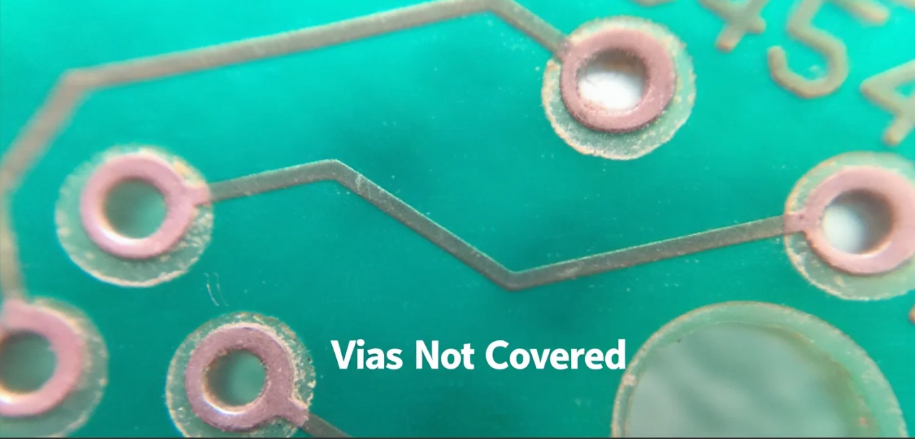
Vias are completely exposed, with the pad copper layer directly exposed, commonly used in test points, heat dissipation designs, or simple PCB designs with low requirements for functionality and quality.
Advantages: Direct contact measurement with probes is possible; heat dissipation capacity is enhanced; no additional processes are required, reducing costs. Simple 1-layer PCB, 2-layer PCB with large line width, line spacing, few holes, and large hole diameter.
Disadvantages: Exposed copper is prone to corrosion by moisture/sweat (copper rust issue); solder paste is likely to flow into the hole during soldering, leading to insufficient solder in Solder joint —without the protection of soldermask ink, improper operations during PCB manufacturing or assembly, such as direct hand contact with the PCB, may cause sweat residue. Poor storage environment of the PCB with high humidity may also lead to moisture corrosion.
Design Recommendations: Avoid use in BGA areas; exposed pads need surface treatment (e.g., ENIG or immersion tin) to enhance oxidation resistance. It is not recommended to use Vias Not Covered if there are many BGA designs.
4. Via Filled with Resin
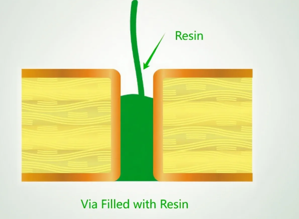
Epoxy or acrylic materials are used to fill vias after electroplating to achieve a high flatness surface. The filling process involves injecting fill material such as non conductive epoxy material or copper epoxy into the via, ensuring complete fill and insulation. It is important to remove excess resin and planarize the hole barrel to achieve a smooth copper surface and proper surface finish for reliable soldering and assembly.
Advantages: Solves the bubble problem of laser blind vias and the via issue in BGA; provides a supporting foundation for subsequent stacked vias; avoids short circuits caused by solder paste infiltration during SMT placement affecting soldering.
Disadvantages: The cost is higher than Tenting Vias and Plugged Vias with Soldermask. However, since only some vias need to be filled with Via Filled with Resin, this part of the cost is controllable. In addition, the manufacturing time of Via Filled with Resin is longer, usually at least one more day than Plugged Vias with Soldermask (for PCB prototype manufacturing).
Process Innovation: Vacuum filling technology ensures no bubbles in deep holes; adding silicon powder to the formula reduces CTE to 30ppm/°C, matching FR-4 substrates. The new process is more suitable for more complex products with higher requirements for PCB quality. This helps to expel resin bubbles and further improve reliability and flatness.
Typical Applications: Motherboards of smartphones, wearable devices, and other miniaturized products; any fine line design requiring Laser Direct Imaging (LDI).
5. Via Filled with Copper
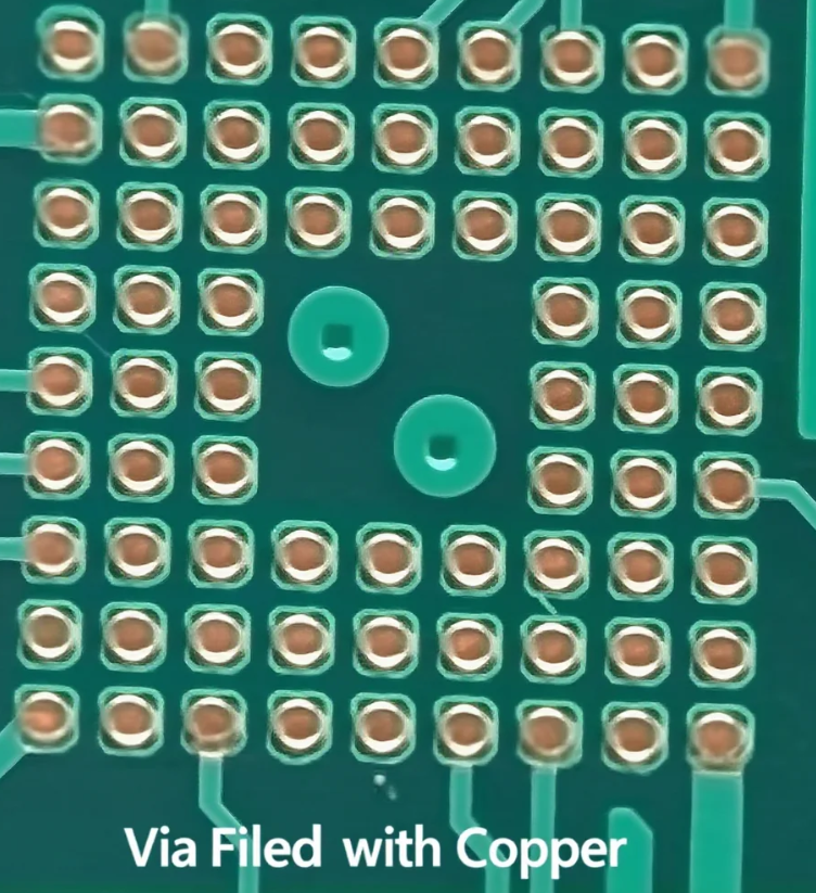
A dense copper layer is deposited in the hole through a special pulse electroplating process, achieving comprehensive improvement in electrical and mechanical properties. The metallic nature of copper as a fill material provides excellent conductivity and thermal management, making conductive filled vias ideal for heat dissipation and enhanced electrical performance in high-reliability applications.
Advantages: The thermal conductivity is as high as 400W/(m·K), more than 10 times better than resin; the current-carrying capacity is increased by 30%-50%; the risk of fracture caused by thermal expansion is eliminated. Since copper is an excellent heat conductor, Via Filled with Copper can effectively help PCB heat dissipation. Moreover, filling the vias with copper also helps to carry larger currents.
Disadvantages: Due to the process characteristics of Via Filled with Copper, this method has a higher cost than all the above methods. Therefore, when choosing Via Filled with Copper, targeted filling can effectively control costs.
Key Processes: Using acidic copper plating solution + organic additives; pulse reverse current to eliminate the “dog bone effect” at the hole mouth; surface grinding to Ra< 0.3μm. Further improve reliability and flatness.
Cost Considerations: The process time increases by 35%; special electroplating lines are required, suitable for high-end server motherboards, automotive electronics, and other fields prioritizing reliability and high-value-added products.
6. Via Filled with Silver
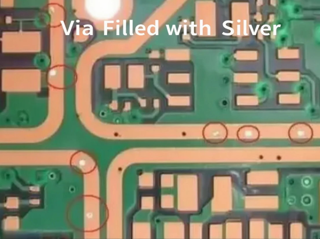
Vias filled with conductive silver paste (Ag-epoxy), balancing conductivity and process simplicity. During the assembly process, proper via fill and surface finish are essential to facilitate reliable soldering of components to solder pads and copper pads, ensuring strong electrical connections and long-term durability.
Advantages: The volume resistivity is about 10⁻⁴Ω·cm, which is not as good as pure copper but much better than non-conductive materials; the curing temperature is only 150°C, avoiding high-temperature deformation. It can be better used in FPC flexible circuits. Suitable for SMT soldering with high-temperature-sensitive materials.
Disadvantages: Via Filled with Silver is not suitable for use in high-temperature operating environments, such as industrial control power supplies, high-power LEDs, and other products prone to high temperatures.
Applicable Scenarios: Dynamic bending areas of flexible printed circuits (FPC); high-temperature-sensitive substrates such as aluminum substrates; RF circuits requiring reduction of skin effect losses.
Process Warnings: The risk of silver migration requires anti-migration formulations; there is compatibility issues with standard immersion silver surface treatment.
Comparison Table of Technical Characteristics of Each Processing Method
Processing Method | Conductivity | Thermal Management | Process Cost | Applicable Scenarios | Surface Flatness |
Tenting | Not required | Poor | ★☆☆ | BGA areas of ordinary consumer electronics | High |
Plugged | Not required | Medium | ★★☆ | Wave-soldered boards | Medium |
Uncovered | High | Excellent | ★☆☆ | Test points/heat dissipation pads | Low |
Resin Filled | Not required | Poor | ★★★ | Laser blind vias in HDI boards | Extremely high |
Copper Filled | Extremely high | Excellent | ★★★★ | Server/AI accelerator cards | High |
Silver Filled | Medium | Good | ★★★☆ | Flexible circuits/RF modules | Medium |
Note: During the filling process, maintaining proper surface tension is crucial to avoid trapped air and ensure complete via fill, which directly impacts the reliability and quality of the finished PCB.
In high-frequency or high-speed designs, the use of bypass capacitors and via in pads is common to minimize inductance and improve signal integrity, supporting optimal performance in advanced electronic circuits.
III. Application Scenarios and Selection Strategies
In >1GHz high-speed links, via parasitic capacitance and inductance become killers of signal integrity. For example, a 0.2mm diameter through via in a 1.6mm thick board generates approximately 0.5pF capacitance and 1.2nH inductance, resulting in a 3.2Ω impedance mutation.
·Optimization Solutions:
Using resin-filled copper vias to reduce capacitive effects; adding ground vias next to signal vias to provide the shortest return path; using Back-drilling to remove useless copper pillars.
High-Density BGA Design
BGA with pitch <0.5mm requires via-in-pad technology:
·Blind and Buried Via Scheme: Directly drilling blind vias from BGA pads to inner layers avoids routing escape difficulties but increases costs by more than 40%.
·Resin Plugging + Electroplating Capping: Through vias are filled with resin under the pad and then surface electroplated with copper to achieve pad flattening.
High-Current Power Paths
The current-carrying capacity of power vias follows the principle of 1A/0.3mm hole diameter. For example, 5A current requires at least 4 parallel 0.3mm vias.
·Optimization Design:
Using copper-filled vias to reduce resistance loss; the anti-pad diameter must be more than 20% larger than the pad diameter to reduce parasitic capacitance.
IV. Key Parameters of Manufacturing Processes
To ensure yield, designs must comply with manufacturers' process limits:
·Minimum hole diameter: 0.3mm (12mil) for mechanical drilling, 0.1mm (4mil) for laser drilling.
·Pad annulus width: ≥0.2mm (8mil) on each side to prevent hole breakage.
·Hole spacing: ≥0.3mm (12mil) to avoid hole wall fracture caused by drilling deviation.
·Aspect ratio: Controlled within 8:1 for conventional boards (e.g., 1.6mm board thickness corresponds to ≥0.2mm hole diameter).
V. Cutting-Edge Trends and Challenges
Via technology is evolving towards nano-scale interconnection and functional integration:
·3D Heterogeneous Integration: Hybrid interconnection of Through-Silicon Vias (TSV) and PCB buried copper vias, achieving chip-substrate collaborative optimization.
·Thermally Conductive Enhanced Materials: Graphene-filled vias reduce thermal resistance by 50%, solving the heat dissipation bottleneck of AI chips.
·Eco-Friendly Process Innovation: Application of cyanide-free copper plating and water-based soldermask ink in via filling processes, reducing toxic waste.
Conclusion
Though small, vias are a key cornerstone of PCB reliability. From consumer electronics to aerospace equipment, the selection of via processing technology needs to find the best balance among signal performance, thermal management, and cost. As 5G millimeter-wave and artificial intelligence hardware place higher demands on circuit density, via technology will continue to evolve towards high integration and multi-functionality. Mastering these core process characteristics will enable engineers to handle high-speed, high-density design challenges with ease.
FAQs
Q: What are the main types of PCB vias and their applicable scenarios?
A:
PCB vias can be divided into three types by structure and function:
·Through Hole: Penetrates the entire PCB, connecting the top layer, bottom layer, and all intermediate wiring layers. It is the most common type of via, suitable for signal or power connection between different wiring layers in multi-layer boards, such as component pin vias in ordinary double-layer boards and interconnection between power layers and signal layers in multi-layer boards.
·Blind Via: Extends only from the top or bottom layer to a specific inner layer without penetrating the entire board. It is suitable for high-density PCB designs to save routing space, commonly used in inter-layer connection of high-speed signals (e.g., DDR, PCIe), and needs to be implemented with laser drilling technology.
·Buried Via: Located inside the PCB, connecting two or more intermediate layers, invisible from the top and bottom layers. It is suitable for scenarios requiring hidden internal connections and improving board surface utilization, such as multi-layer boards (8 layers and above) in mobile phones, drones, and other miniaturized devices, but the manufacturing cost is significantly higher, and drilling and electroplating need to be completed before lamination.
Q: When designing vias, how to determine the appropriate hole diameter and pad size?
A:
The hole diameter and pad size of vias need to be comprehensively determined based on PCB thickness, manufacturing process, and current load:
·Hole diameter selection: The minimum diameter for mechanical drilling is usually 0.2mm (8mil), and laser drilling can be as small as 0.05mm (2mil); power vias need to be calculated according to current (e.g., 1A current recommends a minimum hole diameter of 0.3mm for 1oz copper thickness), while signal vias need to match the wiring width (generally, the hole diameter is not less than 1/2 of the wiring width).
·Pad size: In conventional designs, the pad diameter is 0.4mm-0.6mm larger than the hole diameter (e.g., 0.3mm hole diameter corresponds to 0.7mm-0.9mm pad) to ensure that the pad is not damaged during drilling; for high-density boards (e.g., BGA areas), it can be reduced to 0.2mm-0.3mm larger, but the process capability of the PCB manufacturer needs to be confirmed (to avoid pad detachment).
·Notes: The via spacing must be larger than the hole diameter + 0.2mm to avoid deformation of adjacent vias during drilling; vias near the board edge must be at least 0.5mm away from the board edge to prevent edge cracking.
Q: Do vias have an impact on PCB heat dissipation? How to use vias to enhance heat dissipation effects?
A:
Vias have a significant impact on heat dissipation, and can become efficient heat dissipation channels when designed properly:
·Impact mechanism: Ordinary signal vias, if not specially treated, will have air and insulating layers inside the holes that hinder heat conduction, and may even cause local heating due to parasitic inductance; however, ground vias or vias in large-area copper-clad areas can conduct heat from component pins to the ground layer or heat sink, reducing the temperature of hot spots.
·Heat dissipation enhancement design:
Arrange multiple heat dissipation vias (hole diameter 0.3mm-0.5mm) under the pads of high-power components (e.g., power chips, triodes), directly connecting to the large-area ground copper on the bottom layer, with via spacing of 5mm-10mm to form a "heat dissipation array";
·Use copper paste plugging or full copper electroplating for heat dissipation vias to reduce thermal resistance (the thermal conductivity of copper is about 401W/(m·K), much higher than 0.2W/(m·K) of resin);
·Connect vias directly to component pads (avoiding thin wire connections) to ensure the shortest heat conduction path, such as densely arranging vias on the D pole pad of MOS tubes.
Q: What problems may be caused by excessive number of vias in high-density PCBs? How to control via density?
A:
Excessive number of vias may cause the following problems, and the density needs to be reasonably controlled:
·Process limitations: Excessively high via density (e.g., more than 50 per square centimeter) will lead to insufficient resin filling during PCB lamination, resulting in bubbles or delamination; during drilling, adjacent hole walls are prone to copper layer fracture due to being too thin (less than 0.1mm), affecting conductivity.
·Signal interference: A large number of vias will damage the integrity of the ground layer, forming an "antenna effect", especially in high-frequency signal (e.g., above 10GHz) areas, which may cause crosstalk and EMI radiation.
·Cost increase: The number of vias is positively correlated with the cost of drilling and electroplating processes; the unit price of high-density vias (e.g., laser blind vias) is 3-5 times that of ordinary vias, which will significantly increase the board manufacturing cost.
·Control methods: Prioritize buried vias and blind vias to reduce surface vias; signals of the same network should be routed on the same wiring layer as much as possible to reduce inter-layer vias; power networks use large-area copper cladding instead of parallel connection of multiple vias; confirm the maximum via density with the PCB manufacturer (usually 8-layer boards are recommended to be ≤30 per cm²).
Why PCBMASTER:https://www.pcbmaster.com/why
Join US:https://www.pcbmaster.com/register