Transparent PCB: The Future of Flexible and Clear Circuit Boards
Author:Jack Wang
Introduction to Transparent PCBs
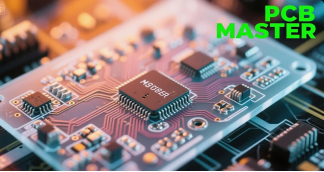
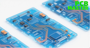
Transparent PCBs, or transparent printed circuit boards, represent a breakthrough in modern electronics by combining the essential functions of traditional circuit boards with the added benefits of transparency and flexibility. Constructed from advanced transparent materials such as glass or ceramic substrates, these innovative circuit boards allow light to pass through while maintaining high electrical performance. This unique feature makes transparent PCBs ideal for applications where both visibility and compact design are critical, such as in automotive displays, medical devices, and next-generation consumer electronics. The use of transparent PCBs offers numerous advantages, including reduced product weight, minimized space requirements, and potential cost savings in manufacturing and assembly. As the demand for sleek, lightweight, and high-performance devices continues to grow, transparent PCBs are becoming widely adopted across industries, driving the evolution of electronic product design and enabling new possibilities in circuit integration and device aesthetics.
Understanding Transparent PCBs
**·**Transparent PCBs are specialized circuit boards that are clear and see-through.
**·**A transparent circuit board is an electronic substrate that allows light to pass through, with visible conductive traces and components.
**·**Transparent PCBs possess properties such as high transparency, excellent flexibility, good conductivity, lightweight, impact resistance, high-temperature resistance, and environmental friendliness. A ceramic substrate can also be used for transparent PCBs, offering higher thermal conductivity but lower optical transmissivity compared to glass.
**·**Transparent PCBs can allow visibility of internal conductive traces, enhancing the overall design. Pads on transparent PCBs can be made fully transparent or remain visible, depending on the manufacturing method.
**·**They break through limitations of traditional colors with thinner designs for compact electronics integration.
**·**Materials like ITO or silver nanowires can be used for transparent traces in PCBs, and glass or ceramic substrates are commonly used, each with different trade-offs in transparency and heat dissipation.
**·**Transparent PCBs have higher DC resistance due to thin traces compared to traditional PCBs.
**·**The presence of components on transparent PCBs reduces overall transparency, making careful design essential for aesthetic purposes.
**·**Using transparent PCBs enhances visual appeal without bulky shells in electronic products. A glass-based solder mask can enhance optical clarity while maintaining thermal performance.
Types of Transparent PCBs
**·**Transparent flexible PCBs are a type of flexible printed circuit board (FPCB) that combine transparency with flex capabilities, allowing bending and adaptation to various shapes for innovative applications.
Flexible circuits and flexible printed circuits are widely used in applications that require both transparency and the ability to flex or bend, such as in automotive, consumer electronics, medical, and industrial devices.
**·**Transparent glass PCBs offer exceptional mechanical strength and thermal performance, expanding their use in high-temperature environments, but they lack the flex found in flexible printed circuit boards.
Transparent Flexible PCBs
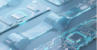
**·**Transparent flexible PCBs utilize advanced materials that allow for both flexibility and transparency, making them suitable for innovative designs. Careful circuit design is essential to ensure both flexibility and transparency in these PCBs.
**·**The materials used in transparent flexible PCBs can withstand high temperatures, with some variants offering thermal resistance up to 260 °C.
**·**Flexible transparent PCBs can achieve around 95% transparency when made with materials like polyester and polyimide.
**·**Unlike traditional PCBs, transparent flexible PCBs are designed to bend and conform to various shapes, enabling innovative product designs.
**·**Transparent flexible PCBs are commonly used in compact devices such as cameras and mobile phones, where space-saving and flexible connections are critical.
Transparent Glass PCBs
**·**Tempered glass is often used instead of ordinary glass in transparent PCBs for enhanced durability.
**·**Glass serves as a substrate option for some transparent PCBs, providing a clear base for electronic components.
**·**Tempered glass is favored for transparent PCBs due to its enhanced durability and ability to absorb shocks.
Transparent glass PCBs also provide reliable electrical connections in high-performance electronic assemblies.
Materials Used in Transparent PCBs
**·**Transparent PCBs are crafted from materials like plastics, glass, or ceramics that allow light to pass through, revealing the circuit elements.
**·**Common materials used include polycarbonate, ceramic, PET, glass-reinforced epoxy, liquid crystal polymer, and PMMA.
**·**Flexible transparent PCBs often utilize polyimide and polyester, achieving up to 95% transparency.
**·**Tempered glass is preferred for transparent PCBs due to its improved durability over standard glass.
**·**Sapphire glass is the most robust material used for high-end transparent PCBs, suitable for extreme environmental conditions.
**·**Aluminum oxide, alumina, and magnesium oxide are commonly used materials in the production of transparent ceramic circuit boards.
**·**Ceramic transparent circuit boards typically exhibit thermal conductivity values ranging from 24 to 31.4 W/mK.
**·**Aluminum oxide, alumina, and magnesium oxide are materials that allow transparent ceramic circuit boards to be used in applications like power LEDs and optical sensors.
**·**Transparent PCBs can have substrates made of glass or ceramics, which facilitate various applications in electronics. The process of creating a hole in transparent PCBs, especially those with glass or ceramic substrates, often requires laser drilling due to the hardness and brittleness of these materials.
Technical Specifications of Transparent PCBs
Transparent PCBs are engineered to meet demanding technical requirements while maintaining their distinctive see-through appearance. The base material typically consists of a transparent substrate, such as tempered glass or high-purity ceramic, which provides both mechanical strength and excellent optical clarity. These substrates are available in various thicknesses, often ranging from 0.2 mm to 2.0 mm, allowing for customization based on application needs. Transparency levels can reach up to 95%, depending on the choice of material and the thickness of the conductive traces.
Conductive pathways are usually formed using ultra-thin copper foil or transparent conductive materials like indium tin oxide (ITO), ensuring reliable signal flow without compromising visibility. The solder mask, available in light green, light blue, or clear finishes, protects the circuit while preserving the board’s transparency. Transparent PCBs are designed to withstand a wide operating temperature range, often from -40°C to 260°C, making them suitable for both industrial and high-performance consumer applications.
Other key technical specifications include high adhesive strength between layers, compatibility with SMT assembly processes, and support for fine-pitch components and complex circuit designs. Minimum order quantities and product weight can be tailored to project requirements, and manufacturers typically accept standard Gerber files for design submission. With their robust technical profile, transparent PCBs deliver reliable performance in demanding environments while enabling innovative, visually striking product designs.
Manufacturing Process of Transparent PCBs
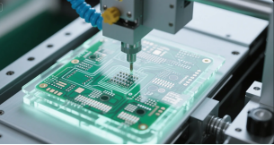
**·**The initial step in creating transparent PCBs involves processing materials such as glass or polyimide to form the base layer.
**·**Applying thin copper layers ensures the creation of conductive pathways while maintaining the board’s clarity.
**·**A photoresist layer is created on the copper layer and exposed to UV light to form the desired circuit pattern.
**·**After etching, a solder mask is applied to protect the circuits and enhance durability during assembly.
**·**Extensive testing is conducted post-manufacturing to ensure the transparent PCB meets clarity and electrical performance standards.
**·**The manufacturing process includes engineering support from a CAM engineer for optimal practices. Higher production volume can help reduce per-unit costs and improve manufacturing efficiency.
**·**Ongoing improvements in material technology aim to reduce the manufacturing costs of transparent PCBs, broadening their accessibility.
**·**Transparent PCB manufacturing can be more costly due to specialized materials, compliance with safety standards, and advanced production processes.
**·**Some manufacturers offer flexible minimum order quantity options, making it easier to prototype or produce small batches of transparent PCBs.
Design Considerations for Transparent PCBs
**·**Understanding the material properties of ceramics, polymers, or glass is essential when designing transparent PCBs.
**·**Transparent PCBs are increasingly used in automotive instrument panels, where both aesthetics and functionality are critical.
**·**Signals can be affected by the materials used, making it important to monitor for interference and impedance matching.
**·**Layer configurations should be optimized with optical performance in mind, potentially requiring consultation with manufacturers.
**·**Designs should account for the unique behavior of transparent materials to avoid issues during manufacturing.
**·**Careful placement of components is necessary to prevent obstructing light from passing through the board.
**·**Hot components should be positioned in areas that won’t overheat the transparent materials. Transparent PCBs are also being integrated into ABS systems in vehicles, where flexible circuits can enhance space-saving and reliability.
**·**A key factor to consider for component layout in transparent PCBs is to avoid blocking light with poor component placement.
**·**Transparent PCBs facilitate easier troubleshooting as visibility of components and circuit traces allows quick identification of issues.
**·**Including test points on the board can facilitate easier testing, given the challenges of visually inspecting transparent PCBs.
**·**Prototyping and testing designs prior to large-scale production is crucial due to the complexities involved.
**·**Collaboration with manufacturers experienced in transparent PCB technology can lead to better design outcomes.
**·**Implementing a clear solder mask enhances both the transparency and protection of the PCB.
**·**Specific guidelines to optimize performance are critical design rules for transparent PCBs.
Applications of Transparent PCBs
·Transparent PCBs are extensively applied across multiple industries due to their unique qualities.
·Transparent PCBs are increasingly employed in consumer electronics for applications like see-through displays and augmented reality devices.
·Transparent PCBs enable visible internal circuitry in smartphones and smartwatches.
·Transparent PCBs are often integrated into compact electronics and wearable devices due to their lightweight and space-efficient design.
·In the medical field, transparent PCBs are utilized in imaging devices and diagnostic equipment.
·Automotive displays benefit from transparent PCBs by providing a sleek appearance without compromising visibility.
·Smart contact lenses are being developed using transparent PCBs for integrating sensors and displays.
Advantages of Transparent PCBs
·The use of transparent PCBs can enhance the visual appeal of electronic devices by allowing light to pass through while maintaining functionality.
·With their sleek appearance, transparent PCBs contribute to the aesthetic appeal of electronic products, making them visually distinctive.
·There is a growing emphasis on enhancing both the aesthetic appeal and functional performance of transparent PCBs.
·These PCBs are not only lighter and thinner but also possess superior optical transmissivity compared to traditional options.
·Transparent PCBs are associated with reduced environmental pollution and lower carbon emissions due to their lighter weight and thinner construction.
Challenges and Limitations of Transparent PCBs
·Transparent PCBs face several challenges and limitations that can hinder their widespread adoption.
·Manufacturing transparent PCBs is often more expensive due to complex processes involved in their production.
·Transparent PCBs frequently experience lower fabrication yields due to challenging material properties, which can increase production costs.
·Thermal management is complicated for transparent PCBs since they cannot utilize traditional heat sinks or multiple thermal vias, leading to potential overheating.
·Repairing transparent PCBs proves difficult, making troubleshooting a more complex task.
·High temperatures during soldering can potentially harm the substrate of transparent PCBs, risking their structural integrity.
·The performance of transparent PCBs can be impacted by their higher electrical resistance, which may affect signal quality in high-frequency applications.
Future Trends in Transparent PCBs
·Future materials suggested for transparent PCBs include hybrid polymers, nanomaterials, and conductive ink.
·Anticipated innovations in the fabrication of transparent PCBs aim to increase yields, reduce production costs, enhance thermal management, add more copper layers, and boost component density.
·Advancements in transparent PCBs are leading to innovative applications in various sectors, including smart devices and automotive electronics.
·The combination of transparent PCBs with flexible designs is expected to create new possibilities in product innovation.
·Transparent PCBs are becoming a focal point in electronic design, driving the evolution of manufacturing technologies.
Environmental Impact of Transparent PCBs
·Transparent PCBs have a smaller carbon footprint due to being thinner and lighter.
·Transparent PCBs reduce material wastage compared to traditional methods, leading to a more efficient manufacturing process.
·The use of bio-based materials, like Soluboard, in transparent PCBs allows for easier recycling and recovery of components.
·Innovations in recycling techniques for transparent PCBs can potentially recover up to 95% of metals, minimizing waste in landfills.
·The ongoing transition towards PFAS-free materials in PCB manufacturing enhances environmental safety by eliminating harmful substances.
How to Order Transparent PCBs
·Select the 'Transparent' option when placing a flexible PCB order.
·When ordering, specifying the type of transparent PCB, whether it be flexible or glass, is essential.
·For orders of transparent PCBs, you can receive a discount of $100 on purchases exceeding $5000.
·OurPCB provides expert manufacturing services for transparent PCBs.
Case Studies of Transparent PCB Implementations
·Transparent PCBs are revolutionizing multiple industries by offering unique transparency and flexibility benefits.
·In the automotive sector, transparent PCBs support innovative features such as heads-up displays and smart windows.
·Healthcare applications include transparent PCBs in wearable medical devices, providing discreet and functional designs.
·Architectural lighting design benefits from transparent PCBs, allowing for modern and cleaner aesthetics in lighting solutions.
FAQs
A. What is a transparent PCB, and how is it different from traditional PCBs?
Q. A transparent PCB is a circuit board with high transparency, which can be used to mount electronic components while maintaining the transparent effect of the circuit parts. Traditional PCBs are usually made of opaque materials such as FR4, metal, or glass fiber, while transparent PCBs use special substrate materials like glass substrates, polyimide (PI) films, PMMA (acrylic), etc., which have higher light transmittance and can meet the needs of products with special appearance requirements. In terms of conductive materials, traditional PCBs commonly use copper foil, whereas transparent PCBs mostly use transparent conductive materials such as ITO, silver nanowires, graphene, etc.
A. What are the main application areas of transparent PCBs?
Q. Transparent PCBs are widely used in high-end electronic product fields such as transparent displays (like transparent TVs, LED transparent displays, transparent light strips, billboards, etc.), smart automotive glass (enabling functional integration on window glass without affecting the line of sight), wearable devices (enhancing aesthetics and wearing comfort), smart home (like invisible touch panels), industrial control (transparent operation interfaces for special equipment), etc.
A. Why is the cost of transparent PCBs higher?
Q. On one hand, the special substrate materials used in transparent PCBs, such as glass substrates, cost 3 to 5 times more than FR-4; even materials relatively commonly used like polyimide films are not cheap. On the other hand, their manufacturing process is complex, requiring special equipment and technology to complete precise etching, lamination, and other operations, all of which increase manufacturing costs.
A. How to test the quality of transparent PCBs?
Q. Visual inspection can be used to look for obvious creases, fractures, bulges, or discoloration; use a multimeter for conductivity testing to detect continuity and resistance of key circuits; utilize X-ray or AOI (Automated Optical Inspection) to detect internal defects like broken lines, layer separation, etc.; environmental simulation testing can also be performed to recreate temperature, humidity, and vibration conditions to verify reliability.
Why PCBMASTER: https://www.pcbmaster.com/why
Join US:https://www.pcbmaster.com/login