Heavy Copper PCBs: PCB Prototype Solutions for Robust Design
Heavy Copper PCBs: PCB Prototype Solutions for Robust Design. Explore heavy copper PCB advantages for demanding applications. Superior thermal management for reliable electronics.
Section 1: Defining Heavy Copper FPCs & Key Technical Parameters
Copper Weight Definition & Range: Within the FPC realm, "heavy-copper" specifically refers to finished copper weights ≥ 3 oz/ft² (approx. 105 μm), extending upwards to 10 oz/ft² (350 μm) and even 20 oz/ft² (700 μm) for extreme applications. This significantly surpasses the standard 1 oz/ft² (35 μm) used in typical FPCs.
Leap in Current-Carrying Capacity: Increased copper thickness directly translates to dramatically higher current capacity. Under identical temperature rise constraints (e.g., ΔT = 10°C), a 1mm wide, 100mm long trace on a 5 oz heavy copper layer can achieve enhanced current-carrying capacity, crucial for the lifespan of the circuit. can reliably handle approximately 15A continuously. An equivalent 1 oz trace typically manages less than 5A – representing a challenge in applications where thermal management is necessary, including PCB design. performance gain exceeding 300%. This directly addresses bottlenecks in high-power-density designs, including considerations for copper thickness also.
Quantifiable Thermal Management Advantage: Copper is an excellent thermal conductor (~400 W/mK). A thick copper layer acts like an integrated heat spreader within the FPC, significantly reducing hot-spot temperatures. Empirical testing confirms that for the same power dissipation (e.g., 5W), a trace on a 5 oz exhibits a peak temperature 15-25°C lower than its 1 oz counterpart. This substantially boosts long-term system reliability and minimizes the need for bulky external heatsinks.
Enhanced Mechanical Robustness: The thick copper layer grants the FPC greater resistance to bending fatigue and improved dimensional stability. In dynamic flexing applications, traces on 3 oz and heavier copper FPCs can endure several times more flex cycles (per standards like IPC-6013) compared to standard FPCs. This makes them particularly well-suited for demanding environments like robotic joint cabling, where pcbs can withstand significant mechanical stress.
Section 2:Heavy copper PCBs The Fine-Line Etching Challenge:
Core Challenge: Etching thick copper demands longer immersion times or stronger etchants, drastically increasing the risk of undercut – where the etchant excessively attacks the copper sidewalls. This causes the actual trace width to become much smaller than designed, ruining precision. Achieving 3 mil (75 μm) line/space on 5 oz copper is exceptionally difficult.
Engineering Solutions: Collaborating with a PCB manufacturer can lead to innovative designs utilizing thicker copper layers.
① Flex PCB designs can benefit from the use of heavy copper for improved thermal management.Pattern Plating over Subtractive Etching: Start with a thin copper base (e.g., 1/3 oz). Apply photolithography to define the circuit pattern with etch resist. Electroplate copper is essential for achieving the desired conductivity of heavy copper in rigid-flex PCB designs. selectively onto exposed areas to reach the target thickness of the copper, including copper thickness also (e.g., 5 oz). Finally, strip the resist. This method minimizes undercut, enabling finer features.
② The use of heavy copper can significantly improve the conductivity of heavy copper circuits.Advanced Etching Processes: Employ high-precision, high-uniformity spray etchers for copper PCB manufacturing. Precisely control the Etch Factor (Etch Depth / Undercut). Target an Etch Factor >3. Utilize etch inhibitors to protect trace sidewalls.
③Design Compensation (Overcompensation): Based on the manufacturer's specific Etch Factor data, intentionally increase the trace width in the design phase to help you design for better performance. This compensates for the expected undercut, ensuring the final etched copper trace meets specifications. Close collaboration with the fabricator is essential for achieving the desired plating process for heavy copper circuit designs.
Lamination Reliability & Delamination Risk:
Core Challenge: Increased copper thickness amplifies the stress generated by the Coefficient of Thermal Expansion (CTE) mismatch between copper and the polyimide (PI) base film or adhesive during thermal cycling (e.g., soldering). This heightens the risk of interfacial delamination, especially with high-Tg materials or multiple reflow cycles.
Engineering Solutions:
①Strategic Material Selection: Prioritize adhesiveless two-layer Flexible Copper Clad Laminate (FCCL), where PI is directly cast onto copper. This offers superior interfacial adhesion, higher thermal resistance (Tg often >250°C), and better CTE matching. If adhesive-based (three-layer) FCCL is used, opt for specialty high-temperature, high-peel-strength adhesives (e.g., modified epoxy or acrylic).
②Surface Treatment Enhancement: Treat the copper surface with Oxide Replacement Treatment (ORT, "browning") or plasma treatment. These processes increase micro-roughness, significantly improving mechanical interlocking and chemical bonding strength with the dielectric. Target Peel Strength ≥ 8 N/mm (IPC-6013 Class 3 requirement).
③Precision Lamination Control: Meticulously control the temperature profile, pressure profile, and vacuum level during lamination. This ensures resin fully flows to fill gaps around thick copper features and eliminates air bubbles. Multi-stage ramp/pressure profiles are critical.
Balancing Rigidity & Flexibility:
Core Challenge: Thick copper significantly increases local stiffness in the FPC. In areas requiring dynamic bending, this can create stress concentration points, leading to fatigue cracks and failure due to insufficient cross-sectional area.
Engineering Solutions:
①Zoned Copper Thickness Design should consider copper thicknesses ranging from standard to heavy copper for optimal performance. Apply heavy copper only the desired copper thickness can ensure optimal current density. where needed for high current or heat dissipation (e.g., connector pads, under power components). Gradually reduce copper thickness (stepped or tapered) in areas requiring flexing. This demands precise localized plating or pre-etching techniques.
②Stress-Relief Geometric Design: help you design for optimal performance. At copper thickness transition zones and bend points, implement features like teardrop pads, large-radius corners, widened traces, and coverlay openings (coordinated with stiffeners) to distribute stress. Avoid traces running perpendicular to the bend axis in flexible printed circuit boards.
③Stiffener Integration: Apply rigid stiffeners (FR-4, aluminum, stainless steel) precisely on the backside of thick-copper areas for support and strain relief. Ensure adjacent bend zones remain free of stiffeners to maintain flexibility, which is vital in applications where pcbs are manufactured for dynamic environments. Achieve smooth rigid-flex transitions.
Section 3:Heavy copper Precision Etching & Plating Control:
①Utilize Vertical Continuous Plating (VCP) lines for high uniformity and low undercut during copper plating, ensuring copper thickness consistency within ±10% to enhance the lifespan of the circuit.
②Implement real-time monitoring of etch rate and chemical concentration during etching. Use automated replenishment systems for bath stability. Post-etch cleaning must be thorough to eliminate corrosive residues, especially in heavy copper plating applications.
Lamination Process Excellence:
①A Vacuum Lamination Press is mandatory for heavy-copper FPCs. High pressure (potentially >300 psi) and temperature, combined with vacuum, are essential to remove interlayer gases and achieve void-free filling and bonding.
②Precisely regulate ramp rates and dwell times to optimize resin flow and ensure complete cure of adhesives or PI.
Rigorous Quality Assurance:
①Automated Optical Inspection (AOI): Perform 100% inspection for defects (opens, shorts, nicks, protrusions) and ensure post-etch trace/space accuracy to maintain the integrity of enhanced current-carrying capacity.
②Microsection Analysis (Cross-Sectioning): Conduct regular sampling to verify copper thickness, undercut, interlayer bond integrity, and hole plating quality.
③Reliability Testing: Subject samples to Thermal Cycling (e.g., -55°C to +125°C, 500 cycles), Thermal Shock, High Temperature/Humidity Storage (e.g., 85°C/85%RH, 1000h), and Flexural Fatigue Testing to validate product lifespan.
Section 4:Heavy copper PCBs use for New Energy Vehicle Powertrains:
①Application: High-voltage sensing/balancing interconnects between Battery Management System (BMS) controllers and modules; gate driver signals and main power current paths within motor inverters (IGBT/SiC modules); power conversion in On-Board Chargers (OBC).
②Value in the thickness of the copper used in manufacturing processes. Heavy-copper FPCs are designed to improve current-carrying capacity and thermal management in high-performance applications, helping you design more efficient circuits. reliably carry hundreds of amps in constrained spaces, withstand under-hood heat/vibration, replace bulky wiring harnesses, and boost system power density and reliability.
Data Center Power Systems:
①Application: Interconnects within high-efficiency server/switch power supplies (e.g., 48V to Point-of-Load converters), Battery Backup Unit (BBU) connections, and heavy copper printed circuit boards.
②Value: help you design for better thermal management. Heavy-copper FPCs Minimize power path impedance in heavy copper PCBs, reduce voltage drop losses, dissipate heat efficiently, and ensure uninterrupted operation of critical infrastructure.
Industrial Automation & Robotics:
①Application: Power and signal transmission within high-power servo drives, industrial robot joint assemblies, heavy machinery control units.
②Value: Heavy-copper FPCs withstand frequent flexing (robot cables), harsh EMI environments, and deliver stable high current where needed.
Aerospace & Defense Electronics:
①Application: Power distribution in radar systems, actuator drives in flight control systems, and power conditioning units in satellites are critical applications where thermal management is essential.
②Value: The high reliability under extreme conditions (cryogenic temperatures, vacuum, radiation) combined with weight savings makes heavy-copper FPCs an ideal solution for circuit board manufacturers.
Section 5: Heavy copper FPCs technology frontiers & Future Evolution
Ultra-Heavy Copper & Hybrid Structures: FPCs with 20 oz+ copper combined with embedded copper inlays offer solutions for kilowatt-class power modules, leveraging the increased current carrying capacity.
Integrated Advanced Thermal Management: Direct integration of heat pipes or vapor chambers within heavy-copper FPC structures enables highly efficient thermal management from chip to system level.
Ongoing Material Innovation: focusing on heavy copper plating for enhanced performance. Flexible substrates with higher thermal conductivity (>5 W/mK), polyimide films with higher glass transition temperature (Tg > 300°C), and lower CTE are continually emerging.
Roll-to-Roll (R2R) Manufacturing Advances: Development of R2R plating and patterning processes suitable for heavy-copper FPCs promises increased production efficiency and reduced costs.
Section 6:Heavy copper FPCs Design Checklist (Core Items)
Conduct Current & Thermal Simulation First: Use simulation tools (e.g., ANSYS Icepak, Cadence Sigrity) to accurately calculate current requirements, temperature rise distribution, and voltage drop. Determine necessary copper weight.
Define Manufacturing Process Route for heavy copper printed circuit boards. Confirm with your fabricator whether pattern plating or subtractive etching will be used for the heavy copper circuit. Understand their specific capabilities (min line/space, max copper weight achievable).
Finalize Material Stackup: Select FCCL type (Adhesiveless / Adhesive-based), base PI film thickness/grade, coverlay material, and stiffener material(s).
Implement Fine-Line Design Rules: Apply etch compensation based on fabricator data; eliminate 90-degree angles; ensure smooth transitions between thick and thin copper zones; apply special rules for critical bend areas.
Ensure Robust Lamination Interface with the appropriate copper foil thickness. Specify copper surface pre-treatment (ORT/Plasma); define required lamination parameters (temp, pressure, vacuum profiles).
Integrate Stiffeners Strategically in rigid-flex PCB designs to enhance structural integrity. Precisely define stiffener locations, shapes, thicknesses, and attachment methods (adhesive type, placement) to ensure optimal performance in copper PCB designs.
Verify DFM Compliance for manufacturing heavy copper designs. Strictly adhere to the fabricator's Design-for-Manufacturability (DFM) guidelines for heavy-copper FPCs, ensuring the core PCB meets specifications for copper thicknesses ranging from standard to heavy copper.).
Plan Comprehensive Reliability Testing: Develop a test plan covering electrical, thermal, mechanical, and environmental stress factors relevant to the application.
Performance Comparison:
Characteristic of the copper board is its ability to handle thicker copper layers for enhanced performance. | Standard FPC (1 oz) | Heavy-Copper FPC (3-10 oz) for enhanced current carrying capacity. | Rigid PCB (2-6 oz) | Key Advantage of Heavy-Copper FPC |
Current Carrying | Low | Very High | High | Far higher current per unit width vs. standard FPC |
Thermal Performance | Poor | Excellent quality in our heavy copper PCBs. | Excellent | Integrated heat spreading path reduces hot spots |
Mechanical Flexibility is crucial when working with types of copper in design, especially in applications where thermal management is a key consideration. | Excellent | Localized / Requires Design | None | Requires zoned copper & structure for rigidity/flex balance |
Fine-Line Capability | Excellent | Challenging | Good | Needs special processes (pattern plating) for fine lines |
Weight | Very Low | Low (vs. Rigid-flex PCB designs are increasingly popular due to their versatility and improved thermal performance. | High | Enables lightweight solutions in power applications |
Space Adaptability | Excellent | Good | Limited | Enables 3D routing in complex spaces, which is crucial in printed circuit board manufacturing. |
Typical Application | Signal, Sensors with enhanced current density thanks to thicker copper layers. | High Current, High Heat, including PCB design considerations. | General Electronics applications often require careful consideration of current-carrying capacity and thermal management. | Solves |
Section 7:Section for heavy copper PCBs FAQ
Q: What’s the minimum line/space achievable on a heavy-copper FPC?
A: This heavily depends on copper weight and process. For 3 oz using pattern plating, 4-5 mil (100-125 μm) is feasible. For 5 oz+, it becomes much harder; much thicker copper in the range of 6-8 mil (150-200 μm) is more typical. Subtractive etching capability is lower. Consult your specific manufacturer.
Q: How much more expensive is a heavy-copper FPC vs. a standard FPC?
A: Cost increases significantly due to: more expensive base materials; complex plating/etching (longer process times, yield challenges); potential need for specialized lamination equipment/processes; stricter QC. Costs are typically 1.5x to 3x+ higher than equivalent standard FPCs, varying by copper weight, complexity, and yield.
Q: Are heavy-copper FPCs reliable in dynamic flexing applications?
A: Using heavy copper directly in areas requiring frequent flexing is NOT recommended, especially when considering copper thickness also. due to fatigue risk. Reliability hinges on design: use thin or stepped copper in dynamic zones; implement stress-relief features (large radii, teardrops); place stiffeners for support near static/heavy copper areas, especially in heavy copper flexible applications. Properly designed, they meet IPC flex standards for printed circuit boards.
Q: How can I ensure lamination reliability in a standard PCB and prevent delamination?
A: Key strategies: Prioritize adhesiveless two-layer FCCL for best PI/copper bond; if using adhesive-based, select high-Tg/high-peel-strength adhesives suitable for heavy copper PCB applications; MUST treat copper surface (ORT/Plasma); use a vacuum lamination press for achieving improved thermal management in multilayer designs. Design with optimized profiles; avoid large copper-free areas within thick-copper zones during design to ensure increased current carrying capacity.
Q: Can you quantify the thermal advantage? How best to leverage the amount of copper for optimal performance?
A: The advantage is significant and quantifiable. Example: Under identical power, a 5 oz trace on a copper foil runs 15-25°C cooler than 1 oz. Leverage it by: Solder power components (MOSFETs, diodes) directly onto heavy-copper areas (acts as heatsink); design thermal paths under/behind copper (e.g., thermal interface material + metal housing); expose copper areas to air/cooling via coverlay openings (where possible). Thermal simulation is crucial.
Conclusion
Heavy-copper FPC engineering represents the convergence of materials science, precision manufacturing, and innovative design. Successfully navigating challenges like etching control, lamination integrity, and the rigidity-flexibility trade-off demands a deep understanding of material properties, process limitations, and failure mechanisms from engineers. As demand surges from 5G, electrification, and AI-driven computing, pcbs are used in a variety of applications that require robust thermal management solutions. will play an indispensable role at the critical intersection of high power delivery and unwavering reliability. Mastering the principles outlined in this guide provides a fundamental advantage in designing the next generation of high-density, high-performance electronic systems.
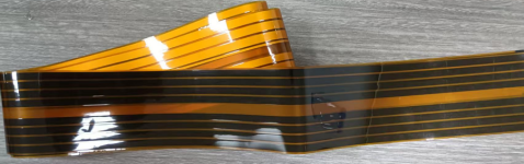
All kinds of FPCS manufactured by PCBMASTER